The Importance of Solder Ball Shear Testing in SMT Reliability
Ball Grid Array (BGA) packages rely on an array of solder balls to form both the mechanical and electrical co
ection between the package substrate and the PCB. Unlike leaded packages where the solder joint geometry provides inherent mechanical robustness, BGA solder balls are relatively small (0.3-0.6 mm diameter) and have a limited cross-sectional area. The shear strength of each solder ball-to-pad interface is the primary determinant of the package’s resistance to mechanical shock, thermal cycling, and vibration.
JESD22-B117 is the JEDEC standard for solder ball shear testing, specifying the test apparatus, sample preparation, shear tool geometry, test speed, and data reporting requirements. For SMT manufacturers, shear testing provides a quantitative measure of joint quality that goes beyond visual inspection and X-ray analysis—it directly measures the mechanical integrity of the metallurgical bond at the copper pad interface.
JESD22-B117 Test Methodology
Shear Test Apparatus and Setup
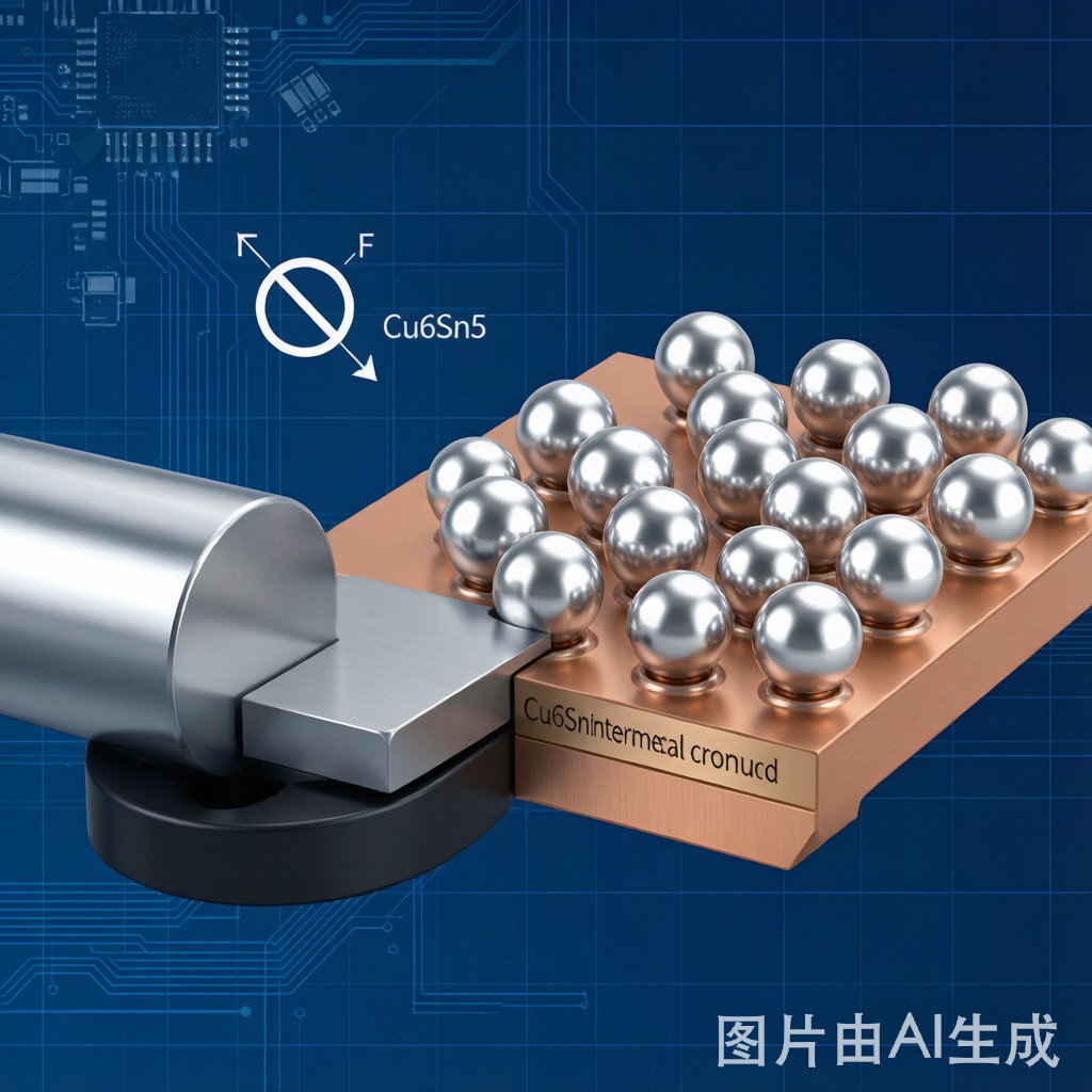
The shear test uses a carbide-tipped shear tool mounted on a motorized stage. The tool is positioned at a defined height above the substrate surface (typically 50-100 micrometers, or 25% of the ball height) and moves horizontally at a constant speed (typically 100-500 micrometers per second) to push the solder ball off the pad. The test records the peak shear force (in grams-force or Newtons) and the force-displacement curve profile.
Key test parameters per JESD22-B117:
- Shear tool height: 50-100 micrometers above the substrate surface. Too low risks contact with the pad; too high produces a peel failure mode rather than shear.
- Shear speed: 100-500 micrometers/second. Higher speeds produce brittle fracture modes; lower speeds produce ductile failure. Use 200 micrometers/second for SAC305 to match field loading conditions.
- Tool clearance: 0.05-0.10 mm between the tool tip and the substrate surface.
- Sample size: Minimum 10 balls per condition, tested from at least 3 different locations on the package.
Sample Preparation
Test samples are actual BGA packages or specially prepared test vehicles with individual solder balls attached to copper pads. For production monitoring, use packages from the same reflow batch as production boards. For process development, prepare dedicated test vehicles with known pad geometries and surface finishes to isolate specific variables.
Minimum Shear Force Requirements
The minimum acceptable shear force depends on the solder ball diameter and the solder alloy. For SAC305 on copper pads with ENIG surface finish:
| Ball Diameter (mm) | Min Shear Force (gf) | Typical Force (gf) | Failing Force (gf) |
|---|---|---|---|
| 0.30 | 350 | 500-800 | < 200 |
| 0.40 | 500 | 700-1100 | < 300 |
| 0.50 | 700 | 1000-1500 | < 450 |
| 0.60 | 900 | 1300-1900 | < 600 |
For SAC105 (lower silver content), typical shear forces are 10-15% lower. For SnPb (tin-lead, legacy), forces are 20-25% lower than SAC305.
Failure Mode Classification and Root Cause Analysis
Mode 1: Ductile Bulk Solder Failure (Desirable)
The solder ball shears through the bulk solder material, leaving a characteristic ductile fracture surface with visible plastic deformation and a rough, dimpled texture. The fracture surface is typically 30-60% of the original ball height. This is the desirable failure mode—it indicates that the solder-pad interface is stronger than the bulk solder, meaning the metallurgical bond is sound.
Shear force: Typically at or above the “typical” values in the table above. Root cause if force is below minimum: Insufficient reflow temperature (below liquidus), insufficient time above liquidus, or solder paste contamination. Correct by optimizing reflow profile and verifying paste condition.
Mode 2: Brittle Interfacial Failure at IMC Layer (Critical Defect)
The solder ball separates cleanly at the interface between the solder and the copper pad (or between the solder and the nickel layer for ENIG pads). The fracture surface is flat, smooth, and shows no ductile deformation. This is the most dangerous failure mode—it indicates a weak or defective intermetallic compound (IMC) layer that will likely fail in field service under thermal cycling or mechanical shock.
The intermetallic layer in SAC305 on copper consists primarily of Cu6Sn5 (eta-phase), with a thi
er Cu3Sn (epsilon-phase) layer adjacent to the copper. The Cu6Sn5 layer grows during reflow and continues to thicken during thermal aging. Excessive IMC thickness (>5 micrometers for Cu6Sn5) makes the interface brittle and reduces shear strength by 30-60%.
Root causes:
- Excessive reflow temperature or time: Peak temperature above 260 degrees C or time above liquidus exceeding 120 seconds produces a thick, brittle Cu6Sn5 layer. Optimize reflow profile to TAL 60-90 seconds at 245-255 degrees C.
- Multiple reflow cycles: Each reflow cycle adds 0.5-1.0 micrometers to the Cu6Sn5 thickness. BGA packages that undergo rework (second reflow) have 30-40% lower shear strength than single-reflow packages.
- Copper pad contamination: Organic contamination (flux residue, fingerprint oils) on the copper pad before reflow creates a localized barrier that prevents IMC formation, producing a weak spot in the interface.
- ENIG black pad: On ENIG pads, excessive phosphorus co-deposition in the nickel layer (>10 wt%) creates a “black pad” defect that produces brittle interfacial fracture at shear forces 40-60% below normal.
- Aging at elevated temperature: Long-term exposure to 125-150 degrees C (common in automotive and industrial applications) accelerates Cu3Sn growth, converting the ductile Cu6Sn5 layer to brittle Cu3Sn and reducing shear strength by 5-15% per 1000 hours of aging.
Mode 3: Pad Cratering (Substrate Failure)
The solder ball remains intact but tears the copper pad and underlying FR4 laminate from the substrate. This failure mode is not a solder joint failure—it is a substrate mechanical failure caused by excessive shear force or weak laminate material. Pad cratering is common on thin PCBs (0.4-0.8 mm) with small pad sizes and high-mass BGA packages.
Root causes: Excessive BGA mass relative to pad area, weak FR4 Tg (below 150 degrees C), insufficient copper adhesion to laminate, or thermal cycling degradation of the laminate. Correct by using high-Tg laminate (Tg > 170 degrees C), increasing pad diameter, or adding underfill to distribute mechanical stress.
Mode 4: Partial Shear (Mixed Mode)
The fracture surface shows a combination of ductile bulk solder failure and brittle interfacial failure. Typically, a portion of the ball shears through the bulk solder while the remainder separates at the IMC interface. This mixed mode indicates inconsistent bonding across the pad surface—some areas have sound metallurgical bonds while others have weak or absent IMC formation.
Root causes: Non-uniform pad surface finish (varying ENIG nickel thickness), uneven solder paste deposition, or localized contamination. Correct by verifying pad surface finish uniformity (XRF thickness mapping) and ensuring consistent paste printing.
Factors Affecting Shear Strength on Copper Pads
Surface Finish Impact
| Surface Finish | Typical Shear Force (0.4mm ball) | Dominant Failure Mode | Reliability Rating |
|---|---|---|---|
| ENIG (3-5um Ni / 0.05um Au) | 700-1100 gf | Ductile (Mode 1) | Good |
| ENEPIG (Ni/Pd/Au) | 750-1150 gf | Ductile (Mode 1) | Excellent |
| OSP (bare copper) | 650-950 gf | Ductile (Mode 1) | Good (if fresh) |
| Immersion Silver | 680-1000 gf | Mixed (Mode 4) | Fair |
| Immersion Tin | 630-920 gf | Mixed (Mode 4) | Fair |
| HASL Lead-Free | 600-880 gf | Ductile (Mode 1) | Good (uneven surface) |
Reflow Profile Impact
The reflow profile directly controls IMC formation and shear strength. Key relationships:
- Peak temperature 245-250 degrees C: Produces 1-2 micrometers Cu6Sn5. Optimal for shear strength. Ductile failure mode.
- Peak temperature 255-260 degrees C: Produces 2-3.5 micrometers Cu6Sn5. Acceptable but approaching the upper limit for ductile behavior.
- Peak temperature >265 degrees C: Produces >4 micrometers Cu6Sn5. Risk of brittle interfacial failure. Shear strength reduced 15-25%.
- Time above liquidus (TAL) 60-90s: Optimal range for SAC305. Provides sufficient time for complete wetting and IMC formation without excessive growth.
- TAL >120s: Excessive IMC growth, 10-20% shear strength reduction. Common in slow conveyor speeds or dual-zone reflow ovens.
Shear Testing for Process Qualification and Monitoring
Shear testing should be performed at three stages of the SMT process lifecycle:
- New process qualification: Test 30 balls (10 per package, 3 packages) after initial reflow to establish baseline shear force and failure mode. All balls must exceed the minimum force and show ductile failure mode (Mode 1).
- Production monitoring: Test 10 balls per shift from production boards. Track the average and minimum shear force on SPC charts. Investigate any reading below the minimum or any shift to brittle failure mode.
- Aging and reliability testing: After thermal cycling (500-1000 cycles, -40 to 125 degrees C per IPC-9701) or high-temperature storage (1000 hours at 125 degrees C), re-test shear strength. Acceptable degradation is <15% reduction from baseline. Greater reduction indicates an aging-induced brittleness problem in the IMC layer.
Conclusion
BGA solder ball shear testing per JESD22-B117 is a powerful tool for evaluating the mechanical integrity of the solder-to-copper pad interface. The test goes beyond visual and X-ray inspection by directly measuring the metallurgical bond strength and identifying the failure mode—ductile bulk solder fracture (desirable) versus brittle interfacial failure (critical defect). The dominant factors controlling shear strength are the reflow profile (which controls IMC thickness), the surface finish quality, and the absence of contamination. By implementing shear testing at process qualification, production monitoring, and reliability testing stages, SMT manufacturers can detect and correct weak interfaces before they become field failures—ensuring that BGA packages survive the mechanical and thermal stresses of real-world deployment.



