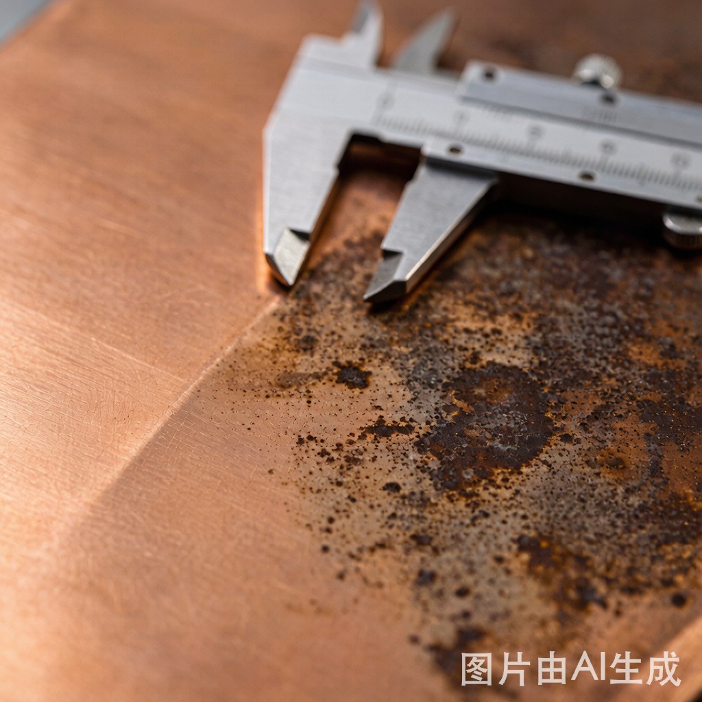
Why Tarnish on Copper Strip Matters for SMT Assembly
Copper strip is the foundational material for SMT component lead frames, EMI shielding clips, and co
ector contacts. In its ideal state, bare copper strip has a bright, reflective surface that solders readily with standard SAC305 paste. However, during storage between manufacturing and SMT assembly, copper undergoes progressive surface oxidation that produces visible tarnish discoloration. What begins as a subtle hue shift can escalate to dark brown or black oxide layers that severely degrade solderability—causing wetting defects, insufficient solder fillets, and field reliability failures.
For electronics manufacturers in Southeast Asia, where ambient humidity routinely exceeds 75% RH and warehouse temperatures reach 35-40 degrees C, copper strip tarnish develops 5-10 times faster than in temperate climates. A coil of bright copper strip stored in an uncontrolled warehouse in Penang or Ho Chi Minh City can develop unacceptable tarnish within 2-4 weeks, compared to 3-6 months in a climate-controlled facility in a temperate zone.
The Oxidation Sequence: Understanding Tarnish Color Stages
Stage 1: Bright Copper (0-24 hours exposure)
Freshly slit or cleaned copper strip has a bright, metallic luster with reflectivity above 80%. At this stage, the surface has only a 2-5 nm native Cu2O (cuprous oxide) layer that is transparent and does not impede solder wetting. Wetting balance tests per J-STD-002 show wetting times of 0.5-1.5 seconds at 245 degrees C with SAC305 solder. This is the ideal starting condition for SMT assembly.
Stage 2: Light Straw to Gold (24-72 hours)
As exposure continues, the Cu2O layer thickens to 10-30 nm and begins to interfere with light, producing a straw-yellow or golden hue. The surface is still solderable with standard flux, though wetting times increase to 1.5-3.0 seconds. This stage is visually detectable but does not require corrective action for most SMT processes.
Stage 3: Brown to Red-Brown (3-7 days)
The oxide layer grows to 50-100 nm, transitioning through orange-red and brown colors. At this thickness, the oxide begins to present a measurable barrier to solder wetting. Wetting times extend to 3-5 seconds, and contact angle increases from the ideal 15-25 degrees to 35-50 degrees. Solder fillets may show partial wetting defects on edges and corners. Recovery action is recommended at this stage.
Stage 4: Dark Brown to Black (1-2 weeks)
CuO (cupric oxide) begins to form on top of the Cu2O layer, producing a dark brown to black surface. The combined oxide thickness reaches 100-500 nm. Solderability is severely degraded: wetting times exceed 5 seconds, and in many cases, complete non-wetting occurs. Contact angles exceed 60 degrees, and solder beads up on the surface rather than spreading. This stage requires aggressive recovery treatment or material scrapping.
Stage 5: Green Patina (weeks to months)
In environments with atmospheric CO2 and moisture, basic copper carbonate (Cu2(OH)2CO3) forms as a green patina. This layer is porous, electrically semi-conductive, and completely blocks solder wetting. Strip at this stage is unsalvageable for SMT use and must be scrapped or remelted.
Solderability Testing Methods
Wetting Balance Test (J-STD-002, Test C)
The wetting balance test is the most quantitative method for evaluating copper strip solderability. A test coupon is immersed in a molten solder bath at 245 degrees C, and the wetting force is recorded over time. Key parameters:
| Parameter | Acceptance Criterion | Failure Indicator |
|---|---|---|
| Wetting time (T0) | < 2.0 seconds | > 5.0 seconds |
| Maximum wetting force (Fmax) | > 0.2 mN/mm | < 0.1 mN/mm |
| Wetting rate (dF/dt) | > 0.15 mN/mm/s | < 0.05 mN/mm/s |
| Contact angle | < 30 degrees | > 45 degrees |
Dip-and-Look Test (J-STD-002, Test A)
For rapid incoming inspection, the dip-and-look test provides a pass/fail assessment. Dip a copper strip coupon in activated flux (RA or RMA type) for 3-5 seconds, then immerse in a 245 degrees C SAC305 solder bath for 5 seconds. Inspect the surface: at least 95% coverage with smooth, shiny solder film indicates acceptable solderability. Any bare copper areas larger than 5% of the total surface area indicate a solderability failure requiring recovery treatment.
Accelerated Tarnish Factors in Southeast Asian Climates
Several environmental factors specific to Southeast Asian manufacturing environments accelerate copper tarnish beyond what temperature and humidity alone would predict:
- Sulfur compounds (H2S, SO2): Industrial zones in Jakarta, Bangkok, and Metro Manila frequently have atmospheric SO2 levels of 5-20 ppb. Even trace H2S (0.5-2 ppb) from nearby industrial processes or volcanic activity produces copper sulfide (Cu2S) at rates 10-20 times faster than clean room conditions. Cu2S is dark and non-wetting.
- Chloride deposition: Coastal locations within 5 km of the ocean experience chloride deposition rates of 10-100 mg/m2/day. Chloride ions penetrate the Cu2O layer and accelerate localized corrosion (pitting), producing dark spots that resist solder wetting even when the surrounding surface appears acceptable.
- Ammonia exposure: Agricultural areas and facilities using ammonia-based refrigerants can expose copper to NH3 levels of 1-5 ppm. Ammonia forms a soluble copper-ammonia complex that strips the protective oxide and accelerates uniform corrosion.
- Cyclic humidity: Day/night humidity swings of 40-60% RH cause condensation cycles on stored copper. Each condensation event deposits a moisture film that dissolves atmospheric contaminants, creating localized corrosion cells. Over 2-3 weeks of cycling, this produces a mottled tarnish pattern that is more damaging to solderability than uniform oxidation.
Tarnish Recovery Methods
Method 1: Vapor Degreasing + Mild Acid Dip
For Stage 2-3 tarnish, vapor degreasing removes organic contamination, followed by a brief immersion in 5-10% citric acid or dilute HCl (3-5% concentration) for 10-30 seconds. The acid dissolves the Cu2O/CuO layer, restoring a bright, solderable surface. After acid treatment, rinse in deionized water and dry immediately with filtered compressed air. This method recovers 90-95% of original solderability but must be followed by immediate use or protective packaging to prevent re-oxidation.
Method 2: Reductive Flux Reflow
For Stage 3-4 tarnish, reductive flux (containing formic acid or oxalic acid as the active ingredient) can reduce CuO back to Cu2O or metallic copper during the reflow process. Apply the reductive flux to the tarnished surface and run through a standard reflow profile at 245-260 degrees C. The reducing atmosphere converts the black CuO to Cu2O, which is more solderable. This method is less effective than acid dipping but can be integrated into the SMT process without a separate recovery step.
Method 3: Mechanical Abrasion
For localized tarnish on stamped component leads, mechanical abrasion with a fiberglass brush or Scotch-Brite pad removes the oxide layer. This method is labor-intensive and suitable only for small batches or rework. After abrasion, the surface must be soldered within 1 hour to prevent re-oxidation.
Method 4: Chemical Conversion Coating
Apply a benzotriazole (BTA) anti-tarnish treatment after acid recovery. BTA forms a 2-5 nm organic passivation layer on copper that inhibits oxide formation for 30-90 days in normal storage conditions. BTA treatment does not interfere with solder wetting when used with activated flux (RA or RMA type). This is the recommended post-recovery treatment for copper strip that will be stored before SMT assembly.
Storage and Handling Best Practices
Preventing tarnish is far more cost-effective than recovering from it. Implement these storage and handling protocols:
- Vacuum-sealed packaging with desiccant: Seal copper strip coils in vacuum bags with silica gel desiccant (1 unit per 0.5 m2 of surface area). This maintains humidity below 10% RH inside the package and extends shelf life to 6-12 months.
- Nitrogen-purged storage cabinets: For opened coils, store in nitrogen-purged cabinets with O2 levels below 1000 ppm and humidity below 20% RH. Opened coils should be consumed within 72 hours.
- FIFO inventory management: Enforce strict first-in-first-out rotation. Copper strip older than 30 days in ambient storage should be inspected for tarnish before use.
- Gloved handling: Require nitrile gloves for all copper strip handling. Fingerprints deposit salts and oils that accelerate localized tarnish.
- Warehouse environmental control: Maintain storage areas at 20-25 degrees C and <40% RH. In Southeast Asian climates without centralized HVAC, use dehumidifiers in storage rooms to control humidity below 50% RH.
Conclusion
Copper strip tarnish is not merely a cosmetic concern—it is a direct indicator of solderability degradation that can cause SMT assembly defects and field reliability failures. The progression from bright copper to black oxide follows a predictable sequence that can be monitored visually, with wetting balance testing providing quantitative verification. In Southeast Asian manufacturing environments, accelerated tarnish from high humidity, sulfur compounds, and chloride deposition demands aggressive storage controls—vacuum packaging, nitrogen cabinets, and FIFO management. When tarnish does occur, acid dip recovery with BTA passivation can restore solderability for Stage 2-3 degradation, while Stage 4-5 material should be scrapped. The cost of prevention (controlled storage) is always less than the cost of recovery (treatment labor, scrap, and field failure risk).



