Why Lead Coplanarity Matters
In surface-mount technology (SMT) assembly, every lead, pin, or pad on a component must make simultaneous contact with the solder paste on the PCB during reflow. When leads are not coplanar—meaning they do not all lie in the same plane parallel to the PCB surface—some leads may float above the solder paste while others bottom out on the board. The result is insufficient solder volume, open joints, or intermittent electrical co
ections that cause field failures and expensive rework.
Copper lead frames are especially susceptible to coplanarity issues because copper’s high thermal conductivity causes rapid heat transfer during stamping, creating differential thermal expansion across the frame. Additionally, the springback characteristics of cold-worked copper alloys (H02/H04 temper) can cause progressive lead height drift as tools wear or as coil tension varies during high-speed progressive die stamping.
Root Causes of Non-Coplanarity
Stamping and Forming Variations
Progressive die stamping involves multiple stations—blanking, piercing, forming, and cutting. Each station introduces slight dimensional variations due to tool wear, press alignment, and material thickness variation. A 0.02 mm difference in forming depth between stations 8 and 12 can translate to 0.05–0.08 mm lead height variation after the final bend. For fine-pitch components (0.5 mm pitch), IPC-A-610 Class 3 requires all leads to be within 0.08 mm of the seating plane, leaving very little tolerance for cumulative stamping errors.
Material and Coil Effects
Copper strip camber (longitudinal curvature) and coil set (residual curvature from winding) cause the strip to feed unevenly through the die, tilting the lead frame relative to the forming tools. This produces a systematic lead height gradient across the frame—typically one side higher than the other. Thickness variation across the coil width (±5% is common for standard tolerances) also affects the final lead height because the forming tools are set for nominal thickness.
Heat Treatment and Stress Relief
Post-stamping stress relief a
ealing (200–300°C for 1–2 hours) reduces residual stress but can also cause thermal distortion if the frames are stacked improperly or heated unevenly. Copper’s high coefficient of thermal expansion (16.5 × 10⁻⁶/°C) means a 50°C temperature gradient across a 20 mm lead frame can create 0.016 mm differential expansion—enough to violate coplanarity limits for fine-pitch devices.
Measurement Methods
Optical 3D Profilometry
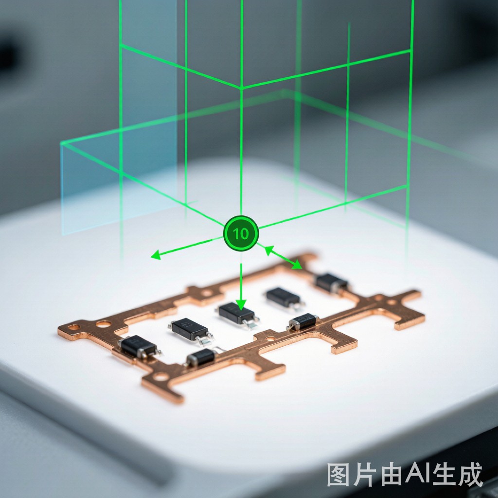
Modern lead frame inspection uses laser triangulation or confocal chromatic sensors to scan the 3D profile of each lead tip. A typical system measures 100–200 leads per frame in under 2 seconds, with height resolution of 0.5 μm and lateral resolution of 5 μm. The software fits a reference plane to the lead tips and reports maximum positive deviation (lead too high), maximum negative deviation (lead too low), and the statistical spread (standard deviation).
Shadow Moiré and Fringe Projection
For high-volume inline inspection, shadow Moiré interferometry projects fringe patterns onto the lead frame and measures fringe distortion to reconstruct the surface topology. This technique is fast (sub-second per frame) and non-contact, but requires controlled vibration isolation. Fringe projection using structured LED illumination offers similar speed with lower sensitivity to ambient vibration, making it suitable for production floors.
Contact Methods: Gauge and FEeler Systems
Legacy contact methods use a precision granite gauge block with a dial indicator or LVDT probe. The lead frame is placed on a flat granite surface, and each lead is pressed gently to measure its deviation from the plane. While accurate, contact methods are slow (20–60 seconds per frame) and risk damaging delicate leads. They are now used primarily for calibration and root-cause analysis rather than production inspection.
Correction and Rework Methods
Coining and Re-Forming
For systematic coplanarity errors (e.g., all leads on the left side are 0.05 mm high), a coining die can be used to re-press the leads into the correct plane. Coining applies localized plastic deformation at the lead bend radii, adjusting the lead angle without affecting the tip geometry. This requires a custom coining tool matched to the lead frame geometry and is typically done as a secondary operation after initial stamping.
Lead Forming and Trim Adjustment
For small random variations, individual lead forming using precision pneumatic or servo-driven forming tools can correct out-of-spec leads. The tool grips the lead body and bends it by a calculated angle to bring the tip into the seating plane. This is practical for low-volume or high-value components but is too slow for mass production of standard commodity lead frames.
Reflow Process Compensation
Some coplanarity errors can be compensated during SMT assembly by increasing solder paste volume or using a stepped stencil. A 0.05 mm lead height difference can be accommodated by applying 0.08–0.10 mm thicker paste on the high leads, but this increases the risk of solder bridging on fine-pitch devices. Alternatively, a flexible solder preform on each pad can accommodate height variations while maintaining joint reliability. These are secondary solutions; the primary fix must be at the lead frame manufacturing stage.
IPC-A-610 Acceptance Criteria
IPC-A-610 defines coplanarity requirements based on component pitch and product class:
- Class 1 (General): Maximum lead height deviation 0.15 mm from the seating plane
- Class 2 (Dedicated Service): Maximum deviation 0.10 mm
- Class 3 (High Performance): Maximum deviation 0.08 mm (or 0.05 mm for fine-pitch ≤0.5 mm)
Leads that exceed these limits are rejected. For copper lead frames in automotive, medical, or aerospace applications where Class 3 is mandatory, coplanarity control is a critical quality gate that must be verified 100% by automated optical inspection (AOI) or 3D profilometry before shipment.
Process Control and Prevention
The most effective approach is prevention through statistical process control in stamping. Monitor and control these parameters:
- Strip thickness variation (Cpk > 1.33 for thickness)
- Die wear (inspect forming radii every 50,000 shots)
- Press parallelism and shut height (check daily with gauge blocks)
- Coil tension and camber (adjust decoiler tension and straightener rollers)
- A
ealing temperature uniformity (thermocouple mapping of the furnace)
Implement a first-article inspection (FAI) protocol for every new coil and every 4-hour production interval. Measure coplanarity on 10 consecutive frames, plot the data on control charts, and adjust the process before limits are exceeded. This proactive approach reduces scrap and rework costs by 70–90% compared to relying solely on end-of-line inspection.
Conclusion
Lead coplanarity is a critical quality parameter for copper lead frames in SMT assembly. Modern 3D optical profilometry enables fast, accurate 100% inspection, while process control in stamping, a
ealing, and material handling prevents non-coplanarity at the source. For high-reliability applications, investing in coining dies and real-time statistical process control pays for itself many times over by eliminating field failures, warranty claims, and rework expenses.



