Introduction
Wide-bandgap semiconductors — silicon carbide (SiC) and gallium nitride (GaN) — are pushing power module operating temperatures beyond 175°C, territory where traditional solder die attach materials reach their reliability limits. Silver sintering has emerged as the leading alternative, offering thermal conductivity 3-5× that of solder and melting points approaching 962°C. For copper lead frame power modules, the transition from solder to sinter requires careful consideration of process compatibility, cost, and long-term reliability.
Why Solder Falls Short at High Temperatures
Traditional die attach solders — typically PbSnAg (high-lead) or SAC305 (lead-free) — have homologous temperatures (ratio of operating temperature to melting point, T/Tm) that become problematic above 150°C. At 175°C operating temperature, SAC305 (Tm = 217°C) operates at T/Tm = 0.87, deep in the creep-dominated regime. This accelerates thermomechanical fatigue, leading to:
- Solder joint coarsening: Intermetallic compounds (IMCs) grow rapidly, embrittling the joint and reducing thermal fatigue life by 50-70% compared to 125°C operation.
- Void coalescence: Micro-voids formed during reflow migrate and merge under thermal cycling, increasing thermal resistance (Rth) by 30-50% over the module lifetime.
- Delamination: CTE mismatch between the silicon die (~2.6 ppm/K), copper lead frame (~17 ppm/K), and solder (~25 ppm/K) creates cyclic shear stress that drives crack propagation.
Silver Sintering Fundamentals
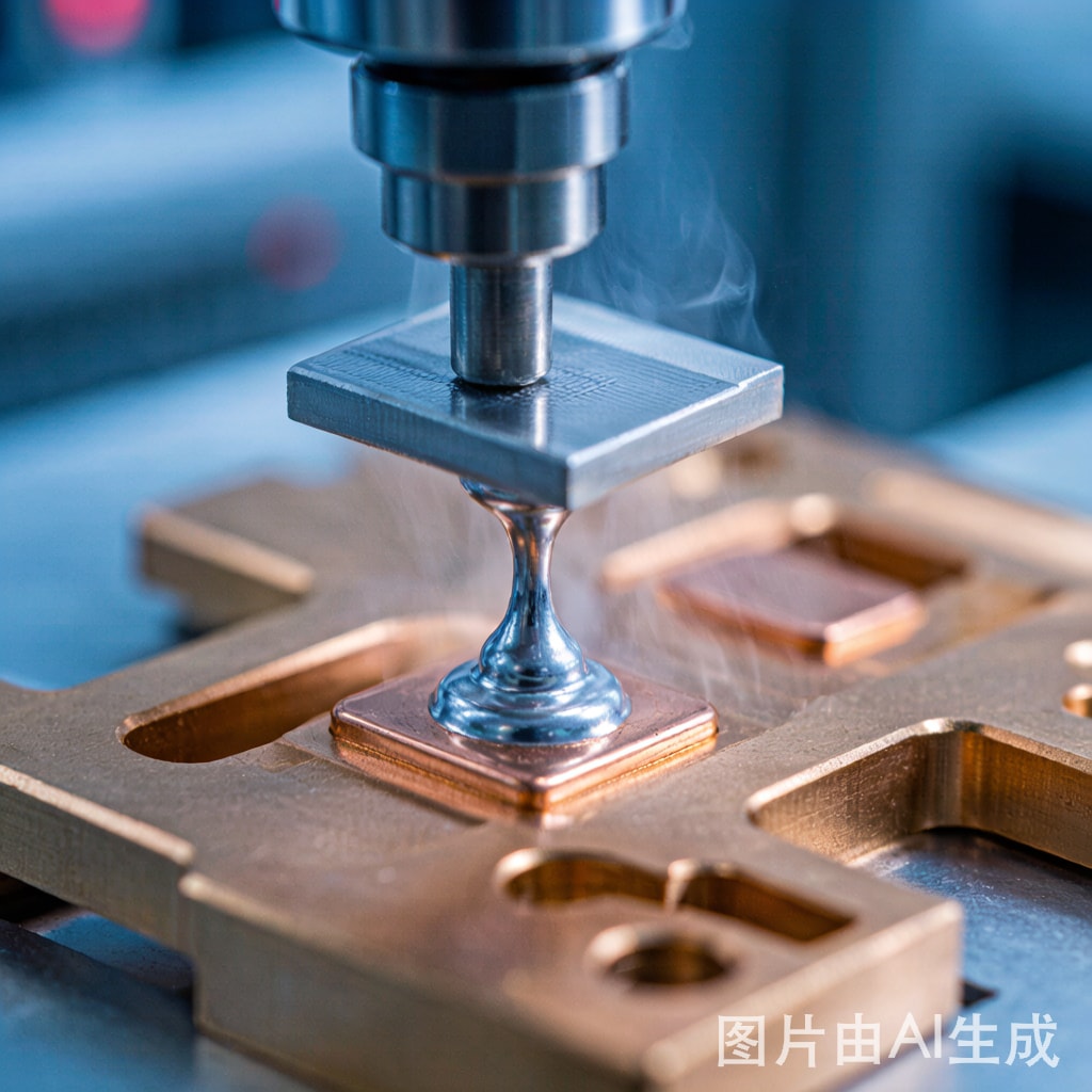
Silver sintering creates a die attach joint by fusing silver particles through solid-state diffusion, typically at 200-280°C — well below silver’s 962°C melting point. The process relies on:
- Silver paste or film: Micron or sub-micron silver particles suspended in an organic binder system. The high surface-area-to-volume ratio of these particles drives the sintering diffusion kinetics.
- Temperature and pressure: Classic pressure-assisted sintering applies 10-40 MPa simultaneously with 230-280°C heat. Pressureless sintering formulations using nanoparticle silver (20-100 nm) can achieve dense joints at 200-250°C without external pressure by leveraging nano-scale surface diffusion.
- Organic burnout: The binder system must completely volatilize before sintering completes, typically requiring a controlled ramp profile with a dwell at 150-200°C for solvent evaporation.
Process Comparison: Sintering vs Soldering
| Parameter | SAC305 Solder | Pressure Sintering | Pressureless Sintering |
|---|---|---|---|
| Processing Temperature | 240-250°C | 230-280°C | 200-250°C |
| Processing Time | 3-5 minutes | 2-5 minutes | 30-60 minutes |
| Applied Pressure | None | 10-40 MPa | None |
| Joint Density | ~100% (voids) | 90-95% | 80-90% |
| Thermal Conductivity | 50-60 W/m·K | 200-250 W/m·K | 100-150 W/m·K |
| Melting Point | 217°C | 962°C | 962°C |
| Die Size Capability | Unlimited | < 100 mm² | Up to 400 mm² |
Copper Lead Frame Surface Preparation
Silver sintering demands a clean, oxide-free copper surface for optimal adhesion. Bare copper oxidizes rapidly at sintering temperatures, forming a Cu₂O/CuO bilayer that inhibits silver diffusion bonding. Two surface preparation approaches are used:
- Silver plating: Electroplating or immersion silver on the copper lead frame die pad provides an ideal silver-to-silver sintering interface. A minimum 2-3 µm silver layer is required to prevent copper diffusion to the sintering interface.
- Forming gas environment: Sintering in N₂/H₂ (95/5%) forming gas reduces copper oxides in-situ, enabling direct sintering to bare copper. This approach eliminates the silver plating step but requires more sophisticated process equipment.
Reliability Testing Results
Published reliability studies comparing silver sintered and soldered die attach on copper lead frames show consistent advantages for sintering:
- Power cycling (ΔTj=150°C): Silver sintered joints survive 50,000-100,000 cycles before 20% Rth increase. Solder joints typically fail at 15,000-25,000 cycles under identical conditions.
- Thermal shock (-55°C to +200°C): Silver sintered joints show minimal degradation after 2,000 cycles. Void area percentage increases by less than 2% absolute. Solder joints show 5-10% void area increase.
- High-temperature storage (250°C, 1,000 hours): Silver sintered joints maintain >90% of initial shear strength. SAC305 solder joints lose >50% shear strength due to IMC overgrowth.
Cost Considerations and Adoption Outlook
Silver sintering paste costs 5-10× more than solder paste per gram, and pressure sintering equipment is significantly more expensive than standard die bonders. However, for SiC and GaN power modules where the semiconductor die cost dominates (>70% of module BOM), the incremental sintering cost is often justified by the 3-4× improvement in power cycling lifetime. Pressureless sintering formulations, while producing slightly less dense joints, are gaining traction for cost-sensitive applications by eliminating the need for specialized press equipment.
Conclusion
Silver sintering is not merely an incremental improvement over solder die attach — it is an enabling technology for next-generation wide-bandgap power modules. The combination of 3-5× higher thermal conductivity, a 962°C effective melting point, and vastly superior thermal cycling reliability makes sintering the clear choice for applications operating above 150°C junction temperature. As SiC and GaN adoption accelerates in electric vehicles, renewable energy, and industrial motor drives, silver sintering on copper lead frames will transition from a specialty process to a mainstream manufacturing requirement.



