Introduction
As electronic devices shrink and mechanical integration demands grow, traditional planar PCBs are increasingly limiting design freedom. Laser Direct Structuring (LDS) offers a compelling alternative: creating copper circuit traces directly on three-dimensional injection-molded plastic substrates, forming what the industry calls 3D-MIDs (Molded Interco
ect Devices). This technology enables ante
as, sensors, co
ectors, and circuit carriers to be integrated into the device housing itself, eliminating separate PCBs and reducing assembly steps.
The LDS Process: How It Works
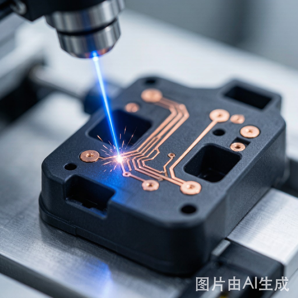
LDS is a three-stage process that transforms a standard injection-molded plastic part into a functional circuit carrier:
- Laser Activation: A focused infrared laser beam (typically 1064 nm wavelength) scans the 3D plastic surface following the desired circuit pattern. The plastic contains a special LDS additive — typically a metal-organic palladium or copper compound — that is activated (cracked open) by the laser’s thermal energy. The activated areas become catalytic seeds for subsequent copper plating.
- Electroless Copper Plating: The laser-activated part is immersed in an electroless copper plating bath. Copper ions in the solution are reduced at the catalytic sites, depositing a uniform copper layer of 5-8 µm thickness. This forms the conductive circuit traces directly on the plastic surface.
- Electrolytic Copper Build-Up and Finish Plating: For higher current-carrying capacity, additional copper is deposited electrolytically to achieve 15-35 µm thickness. A final surface finish — typically ENIG (Electroless Nickel Immersion Gold) or immersion tin — is applied to protect the copper and ensure solderability for SMT component attachment.
LDS-Compatible Materials
Not all plastics are suitable for LDS. The base polymer must withstand both the laser activation temperature and the electroless plating chemistry (typically operating at pH 12-13 and 45-55°C). The most common LDS-grade materials include:
- LCP (Liquid Crystal Polymer): Best-in-class for LDS applications. High heat deflection temperature (280-310°C) allows it to survive lead-free SMT reflow. Excellent chemical resistance for plating baths. Dominates high-frequency ante
a applications.
- PA 4.6 and PA 6.6 (Polyamide/Nylon): Good mechanical properties and lower cost than LCP. Suitable for structural 3D-MID parts but requires careful moisture management before reflow soldering.
- PPA (Polyphthalamide): High-temperature nylon with HDT around 280°C. Compromise between LCP performance and PA cost.
- PC/ABS Blends: Economical option for lower-temperature applications (HDT ~110-130°C). Suitable for low-temperature solder pastes or conductive adhesive assembly rather than traditional SAC305 reflow.
Design Rules for LDS Circuits
LDS circuit design follows rules similar to flexible PCB design but with additional 3D considerations:
- Minimum trace width/space: 150 µm / 150 µm with standard LDS systems. Advanced systems achieve 100 µm / 100 µm. Wider than PCB etching limits but sufficient for most SMT applications.
- Minimum bend radius: Traces crossing 3D contours should maintain a minimum bend radius of 0.5 mm on convex surfaces and 1.0 mm on concave surfaces to prevent copper cracking.
- Via formation: Through-holes can be laser-drilled and metallized as part of the LDS process, but aspect ratios should not exceed 1:1 (diameter:depth) for reliable plating coverage.
- SMT pad design: Pads should incorporate teardrop transitions where traces meet pads to reduce stress concentration during thermal cycling. Extend pads 0.2 mm beyond the component footprint to accommodate LDS trace registration tolerances.
Copper Plating Quality and Adhesion
The Achilles’ heel of LDS circuits has historically been copper-to-plastic adhesion. The electroless copper must form a mechanical bond with the laser-roughened plastic surface. Adhesion is measured using a 90-degree peel test per IPC-TM-650 Method 2.4.9:
- Minimum acceptable peel strength: 0.8 N/mm for general applications, 1.2 N/mm for automotive and high-reliability applications.
- Best-in-class LCP systems: Achieve 1.5-2.0 N/mm peel strength, approaching traditional PCB copper-clad laminate values.
- Adhesion degradation: After 1,000 hours at 85°C/85% RH, LDS copper adhesion typically degrades 15-25%. Design margins must account for end-of-life adhesion, not just initial values.
Applications Driving LDS Adoption
LDS technology has moved beyond its origins in mobile phone ante
as to broader applications:
- Automotive sensors: 3D-MID housings with integrated circuits for LiDAR, radar, and camera modules. Eliminates flex circuits and co
ectors in tight spaces.
- Medical devices: Hearing aids, insulin pumps, and surgical instruments where miniaturization and hermetic sealing are critical.
- LED lighting: 3D circuit carriers that serve as both heatsink and electrical interco
ect for high-power LED arrays.
- Consumer wearables: Smartwatch frames and earbud housings with integrated ante
a and sensor circuits.
SMT Assembly Considerations
Assembling SMT components onto LDS circuits requires several process adaptations. The plastic substrate’s lower thermal conductivity compared to FR-4 means reflow profiles need adjustment — typically a 5-10°C lower peak temperature and 10-15 seconds longer soak time. Solder paste printing on 3D surfaces requires conformal stencils or jet dispensing. For fine-pitch components below 0.5 mm pitch, the wider LDS trace tolerances may require relaxed design rules compared to rigid PCBs.
Conclusion
Laser Direct Structuring represents a paradigm shift in electronic circuit fabrication, moving from the traditional “PCB inside a housing” model to circuits that are integral to the product structure. For applications demanding space savings, reduced part count, and 3D design freedom, LDS copper metallization on LCP or high-temperature nylon substrates delivers reliable SMT-compatible circuits. As automotive, medical, and wearable electronics continue to shrink, LDS adoption will accelerate, driven by its unique ability to merge mechanical and electrical functions into a single molded component.



