Introduction
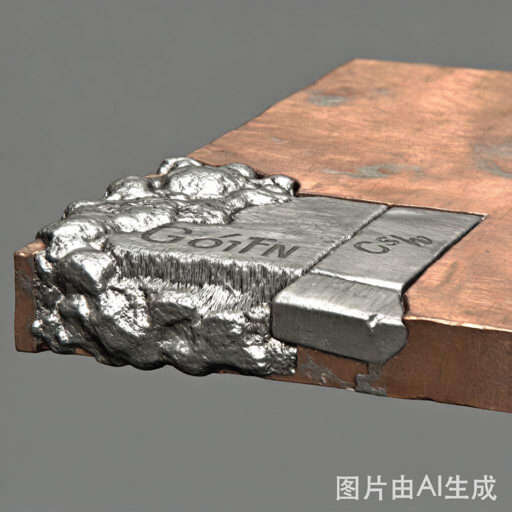
When SAC305 solder alloy melts against a bare copper pad, the two metals do not simply stick together. They react to form intermetallic compounds at the interface. These compounds, primarily Cu6Sn5 and Cu3Sn, are essential for bonding because they create a metallurgical co
ection between the solder and the copper. However, excessive or brittle intermetallic growth can weaken joints over time, especially under thermal aging and cycling. Understanding IMC formation is critical for predicting the long-term reliability of lead-free SMT assemblies on bare copper.
The Chemistry of IMC Formation
During reflow, molten SAC305 solder dissolves copper from the pad surface. Tin from the solder reacts with copper to form Cu6Sn5, the first intermetallic layer. This layer appears as scalloped grains at the solder-to-copper boundary and provides the initial mechanical and electrical co
ection. As the joint ages at elevated temperatures, Cu6Sn5 continues to grow and a thi
er Cu3Sn layer forms between the Cu6Sn5 and the remaining copper pad.
The total IMC thickness increases with time and temperature according to diffusion-controlled growth kinetics. In storage at 125°C, the combined IMC layer can grow from less than 1 µm after reflow to several micrometers after 1,000 hours. Because Cu3Sn is more brittle than Cu6Sn5, thick IMC layers are associated with reduced mechanical toughness and increased susceptibility to thermal fatigue.
Factors That Influence IMC Growth
Several process and material variables control how quickly IMC grows. Reflow peak temperature and time above liquidus determine the initial IMC thickness. Higher peak temperatures and longer liquidus times dissolve more copper and create a thicker starting layer. Multiple reflow cycles, such as those used for double-sided assemblies, add to this growth.
Copper alloy composition also matters. Pure copper pads, such as those used with bare copper strip components or printed circuit board traces, tend to form well-defined IMC layers. Alloying elements like nickel, when present as an underplate, slow IMC growth by creating a diffusion barrier. This is one reason nickel-barrier surface finishes are popular for high-reliability applications.
Typical IMC Thickness Ranges
| Condition | Cu6Sn5 Thickness | Cu3Sn Thickness |
|---|---|---|
| After Reflow | 0.5 – 1.5 µm | Negligible |
| Aged 500 h at 125°C | 2 – 4 µm | 0.2 – 0.5 µm |
| Aged 1000 h at 150°C | 4 – 8 µm | 1 – 2 µm |
| Acceptable Limit | < 5 µm | < 1 µm |
Reliability Implications
IMC layers are inherently brittle compared with solder alloy. When a joint is subjected to thermal cycling, strain concentrates at the interface between the soft solder and the hard intermetallic. A thick or irregular IMC layer provides more crack initiation sites and a weaker path for crack propagation. This is especially important for large components, power devices, and assemblies exposed to automotive under-hood temperatures.
Kirkendall voids are another concern. These small voids form near the Cu3Sn layer due to unequal diffusion rates of copper and tin. Under prolonged high-temperature aging, Kirkendall voiding can reduce the effective bond area and lower fracture strength. The risk is higher for joints on bare copper without a nickel barrier because copper diffuses more freely into tin.
Process Optimization Strategies
Controlling IMC growth starts with optimizing the reflow profile. Use the lowest peak temperature and shortest time above liquidus that still achieves good wetting. Avoid u
ecessary rework and multiple reflow passes. For double-sided boards, minimize the cumulative thermal exposure seen by the first-side joints.
For applications requiring extended high-temperature life, consider surface finishes that slow IMC growth. Electroless nickel immersion gold, electroless nickel electroless palladium immersion gold, and nickel-palladium-gold finishes all provide a nickel diffusion barrier. On bare copper designs, ensure the copper surface is clean and free of oxide, since oxide disruption can create uneven IMC formation and localized thickening.
Inspection and Failure Analysis
IMC thickness is typically measured by cross-sectioning solder joints and examining them with a sca
ing electron microscope equipped with energy-dispersive X-ray spectroscopy. Backscatter electron imaging clearly shows the contrast between solder, Cu6Sn5, and Cu3Sn layers. EDS confirms the elemental composition of each phase.
For production monitoring, pull and shear testing of solder joints provides an indirect measure of interface quality. A declining trend in mechanical strength after aging often indicates excessive IMC growth even before microscopy is performed. Combining mechanical testing with periodic microscopy gives the most complete picture of joint health.
Conclusion
Intermetallic compound growth in SAC305 solder joints on bare copper is unavoidable, but it can be managed. By controlling reflow thermal exposure, selecting appropriate surface finishes, and monitoring IMC thickness through microscopy and mechanical testing, manufacturers can ensure that solder joints retain their strength and reliability throughout the product lifecycle. Understanding IMC behavior is essential for designing lead-free assemblies that perform under demanding thermal and mechanical conditions.



