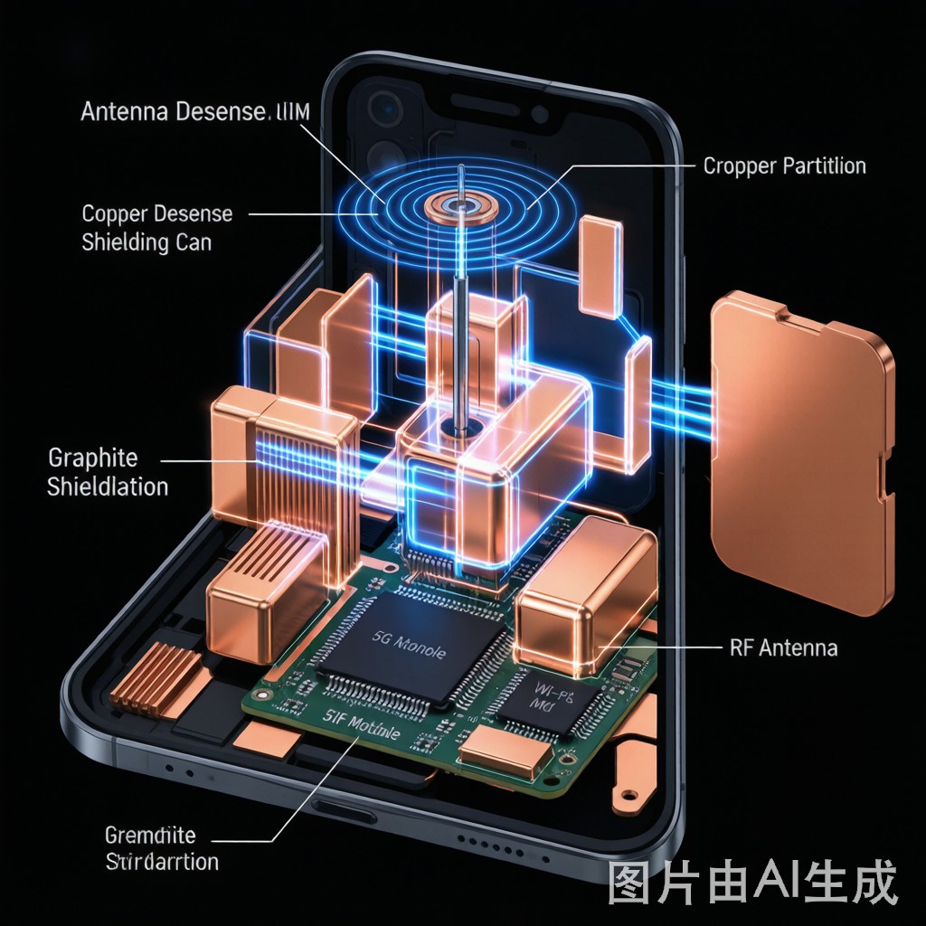
Introduction
Modern 5G smartphones and IoT devices pack multiple radios, high-speed processors, and sensitive ante
as into extremely small volumes. When digital noise from a power management integrated circuit or memory module couples into an ante
a, it raises the noise floor and degrades receiver sensitivity. This phenomenon, known as ante
a desense, is one of the most challenging electromagnetic compatibility problems in compact wireless design. EMI shielding partitions offer a practical way to isolate noise sources from ante
as without increasing overall device thickness.
Understanding Ante
a Desense
Ante
a desense occurs when unwanted electromagnetic energy from an internal source reaches the ante
a port and adds to the received signal. The desense is usually quantified as the increase in ante
a noise figure or the reduction in receiver sensitivity in decibels. A desense level of just 1 dB can significantly reduce data throughput and coverage, especially in weak-signal environments.
Common desense sources include switching regulators, display drivers, camera modules, and high-speed digital buses. The coupling path can be conductive through the PCB ground, radiated through free space, or a combination of both. Because ante
as must remain exposed to the outside world, shielding the noise source is usually more practical than shielding the ante
a.
Role of EMI Shielding Partitions
EMI shielding partitions are conductive walls, often made of stamped copper, nickel-silver, or stainless steel, that create isolated compartments on the PCB. Unlike a full shielding can that covers an entire device, partitions are placed strategically between a noise source and a sensitive ante
a to block the direct coupling path. They work by reflecting and absorbing electromagnetic energy before it reaches the ante
a aperture.
Partitions can be standalone walls soldered to the PCB ground plane, or they can be integrated with shielding cans as part of a compartmentalized enclosure. The key design parameters are height, material conductivity, seam continuity, and grounding impedance. A partition that is not well bonded to the ground plane becomes an ineffective radiator rather than a shield.
Partition Layout Strategies
Effective partition layout begins with identifying the dominant coupling path. If the noise couples primarily through the PCB ground, a partition placed perpendicular to the current path can interrupt common-mode return currents. If the coupling is radiated, the partition should block the line-of-sight between the source and the ante
a while minimizing reflections toward other sensitive circuits.
In practice, engineers often use a combination of full shielding cans for the noisiest components and partial partitions to guide energy away from ante
as. Slots and apertures in partitions must be smaller than the wavelength of the highest frequency of concern. At 5G sub-6 GHz frequencies, this means slot widths below a few millimeters. For millimeter-wave devices, even smaller openings are required.
Common Partition Materials and Properties
| Material | Conductivity | Magnetic | Best Use Case |
|---|---|---|---|
| Beryllium Copper | Excellent | No | Spring fingers and removable shields |
| Nickel-Silver C7521 | Good | No | Corrosion-resistant partitions |
| Stainless Steel 304 | Moderate | No | Structural shields in harsh environments |
| Mu-Metal | Moderate | Yes | Low-frequency magnetic field isolation |
Grounding and Seam Design
A shielding partition is only as good as its co
ection to the reference ground. Soldered co
ections provide the lowest impedance and best shielding effectiveness, but they make rework difficult. Spring fingers and compression contacts allow removable partitions but require careful force management to maintain contact over temperature and vibration cycles.
Seams between partitions and the PCB or shielding can must be continuous. Long, straight seams can act as slot ante
as if the seam length approaches half a wavelength. Stitching the seam with closely spaced ground vias, solder points, or conductive gaskets reduces this risk. The goal is to create a Faraday-like enclosure around the noise source with no significant leakage paths.
Measurement and Validation
Ante
a desense is validated by measuring receiver sensitivity with the offending circuit active and inactive. The difference in sensitivity is the desense level. Engineers typically test in an anechoic chamber with a calibrated communication tester to isolate radiated effects from conducted effects.
Shielding effectiveness of partitions can be evaluated using near-field probes, network analyzers with custom fixtures, or full-wave electromagnetic simulation. Simulation tools such as Ansys HFSS or CST Studio Suite can predict coupling paths and optimize partition placement before physical prototypes are built.
Conclusion
Ante
a desense mitigation in 5G devices requires more than adding shielding cans. It demands a systematic approach to identifying noise sources, mapping coupling paths, and placing conductive partitions where they interrupt the dominant energy flow. With proper material selection, grounding, and validation, EMI shielding partitions enable compact wireless devices to achieve the RF coexistence performance that dense 5G integration requires.



