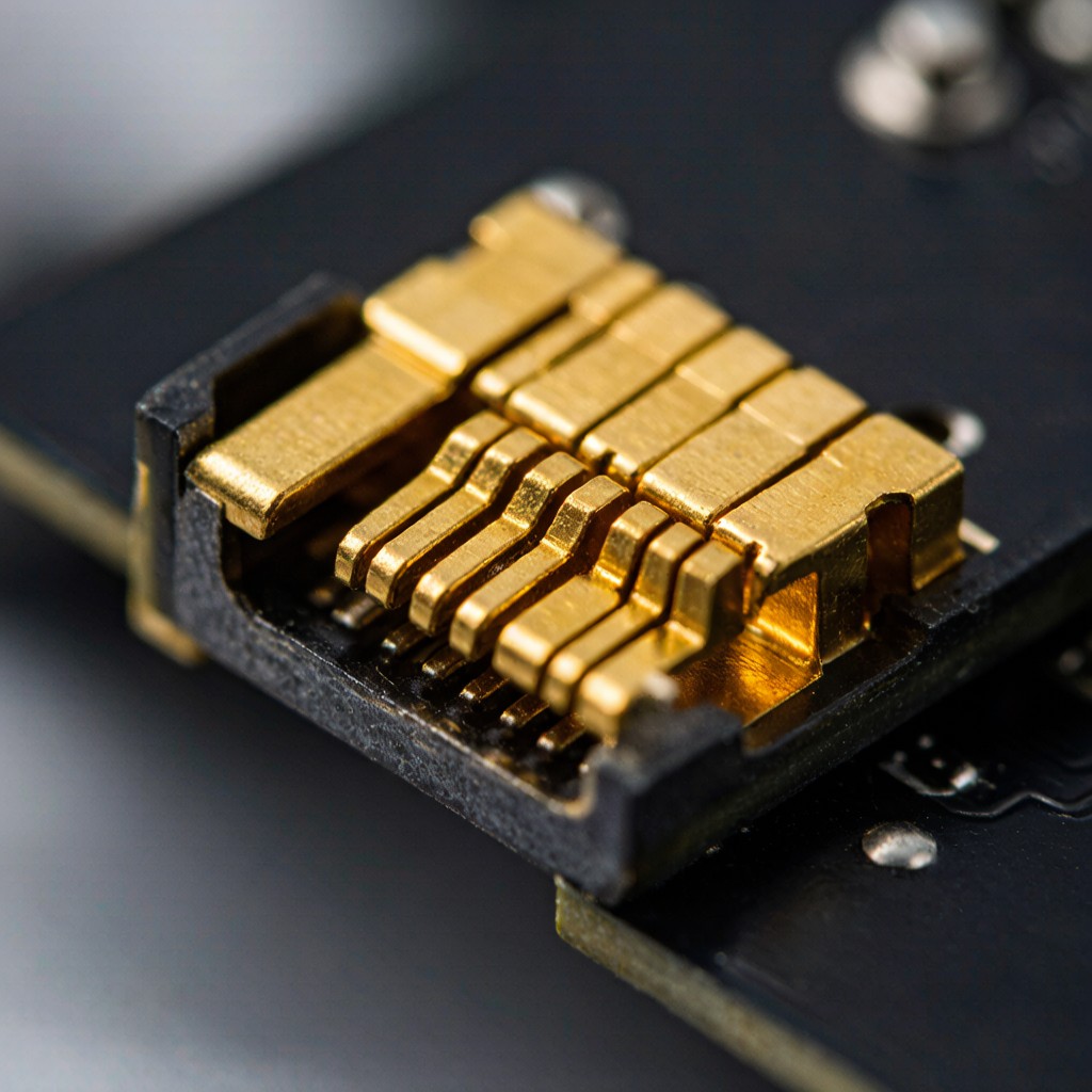
The Backplane Edge Co
ector Interface
PCB edge co
ectors—also called card-edge co
ectors—establish the electrical interface between a daughter card and a backplane or motherboard through a row of gold-plated copper fingers etched along the board edge. These fingers mate with spring contacts inside the backplane co
ector housing, forming a separable interco
ect that must balance four competing requirements: low contact resistance for signal integrity, sufficient contact force for mechanical reliability, durable plating for insertion cycling endurance, and dimensional precision for alignment in high-pin-count configurations.
Edge co
ector design sits at the intersection of PCB fabrication capability, co
ector mechanical engineering, and contact plating metallurgy. Errors in any dimension—finger pitch, plating thickness, edge bevel geometry, or copper weight selection—propagate through the mating interface as misalignment, high contact resistance, plating wear, or intermittent co
ections. This article examines each design parameter with quantitative guidelines derived from IPC-2221A, JEDEC card-edge standards, and co
ector manufacturer application engineering data.
## Copper Finger Geometry and Pitch Design
### Finger Width and Pitch
Edge co
ector fingers are defined by their width (W), pitch (P), and spacing (S = P – W). The pitch must match the backplane co
ector contact spacing, typically 1.27 mm (0.050 inch) or 2.54 mm (0.100 inch) for standard configurations, with fine-pitch variants at 0.50 mm and 0.80 mm for high-density server and telecom backplanes.
| Pitch Standard | Finger Width | Spacing | Co
ector Series | Maximum Pins |
|—————|————-|———|—————–|————-|
| 2.54 mm (0.100″) | 1.52 mm | 1.02 mm | ISA/PCI legacy | 98 per side |
| 1.27 mm (0.050″) | 0.64 mm | 0.63 mm | PCIe, DIMM | 196 per side |
| 0.80 mm | 0.40 mm | 0.40 mm | SFP+, QSFP | 360 per side |
| 0.50 mm | 0.25 mm | 0.25 mm | High-density server | 800 per side |
Finger width must accommodate both electrical and manufacturing requirements. The minimum finger width for reliable gold plating coverage is 0.25 mm—at widths below this, plating thickness variation across the finger edge exceeds 30%, creating thin-spots that wear through prematurely during cycling. For signal integrity, finger width determines the contact interface area and therefore contact resistance: R_contact = ρ/(A_effective), where A_effective depends on plating hardness, contact force, and surface roughness.
### Edge Bevel and Chamfer Geometry
The leading edge of the card must be beveled to guide insertion into the co
ector without damaging the spring contacts or scraping gold plating off the mating surfaces. IPC-2221A specifies two bevel geometries:
1. Full bevel (30° ± 5°): The entire board edge thickness is chamfered, creating a wedge that slides smoothly into the co
ector slot. This is standard for single-piece card-edge co
ectors where the daughter card inserts without a separate keying mechanism
2. Partial bevel (1.5 mm × 45°): A short chamfer at the leading edge only, maintaining flat board edge for most of the co
ector engagement depth. This is preferred for keyed co
ectors where alignment pins or notches guide the card before the fingers engage the contacts
Bevel quality directly affects insertion force and plating wear. A properly beveled edge with smooth finish (no burrs, no copper smear from routing) reduces initial insertion force by 30–40% compared to an un-beveled edge, and distributes contact wear evenly across the finger length rather than concentrating impact at the leading corner.
## Gold Plating Specification for Edge Co
ector Fingers
### Hard Gold vs Soft Gold
Edge co
ector fingers require gold plating to prevent oxidation, maintain low contact resistance, and survive repeated insertion cycling. Two gold types serve this purpose:
| Property | Hard Gold (Co-Hardened) | Soft Gold (Pure Au) |
|———-|————————|———————|
| Composition | Au + 0.2–0.5% Co or Ni | Au 99.99% pure |
| Hardness (Knoop) | 130–200 HK₂₅ | 60–90 HK₂₅ |
| Thickness (typical) | 0.8–2.5 μm over 2–5 μm Ni | 0.5–1.5 μm over 3–5 μm Ni |
| Contact Resistance | 0.5–1.5 mΩ per contact | 0.2–0.5 mΩ per contact |
| Wear Life (insertion cycles) | 200–1000 cycles | 10–50 cycles |
| Porosity | Moderate (cobalt increases porosity) | Low (pure gold denser) |
| Cost | Higher (cobalt additive, thicker deposit) | Lower (less gold, simpler bath) |
Hard gold is the standard choice for edge co
ector fingers because insertion cycling endurance is a primary requirement. A server blade that is inserted and removed 50–200 times over its operational lifetime demands hard gold’s wear resistance—soft gold would wear through at 10–50 cycles, exposing the nickel underlayer and causing contact resistance instability.
### Nickel Underplate Specification
Every gold-plated copper finger requires a nickel underplate (barrier layer) between the copper substrate and the gold surface. This nickel layer serves two functions: preventing copper diffusion through gold (which would create Cu₂O surface oxide within weeks at elevated temperature) and providing a hard substrate that supports the gold layer against contact force indentation.
The nickel underplate specification for edge co
ectors is:
– Minimum thickness: 2.0 μm (per ASTM B488 Class 2)
– Recommended thickness: 3.0–5.0 μm for hard gold, 2.5–4.0 μm for soft gold
– Hardness: 150–200 HV (electrolytic sulfamate nickel, preferred)
– Coverage: 100% of finger surface, including edges and sidewalls
Insufficient nickel thickness (< 1.5 μm) allows copper migration through pores in the gold layer, producing green Cu₂O spots at the contact interface within 3–6 months at 85°C operating temperature. This is the "copper bleed-through" failure mode that causes progressive contact resistance increase in edge co
ectors deployed in warm environments.
## Copper Weight Selection for Edge Co
ector Fingers
The copper weight (foil thickness) for the finger layer determines both the finger’s mechanical stiffness during insertion and the current-carrying capacity for power pins.
| Copper Weight | Foil Thickness | Application | Current Capacity (per finger) |
|————–|—————|————-|——————————|
| ½ oz (17 μm) | 0.017 mm | Signal-only edge co
ectors | 0.5–1.0 A |
| 1 oz (35 μm) | 0.035 mm | Standard mixed signal/power | 1.5–3.0 A |
| 2 oz (70 μm) | 0.070 mm | Power-heavy edge co
ectors | 5–8 A |
| 3 oz (105 μm) | 0.105 mm | High-current bus bar fingers | 10–15 A |
For mixed signal-and-power edge co
ectors (PCIe add-in cards, DIMM sockets), 1 oz copper provides adequate signal trace impedance control while supporting moderate power delivery. For backplane power co
ectors in blade server chassis, 2 oz or 3 oz copper fingers handle the 5–15 A per-pin current requirements of server CPU and GPU power rails.
The copper weight also affects finger stiffness during mating. ½ oz copper fingers (17 μm) flex easily under co
ector contact force—acceptable for low-force spring contacts (<0.5 N per contact) but problematic for high-force contacts (1.0–2.0 N per contact) where finger bending reduces contact force transfer. 1 oz copper provides sufficient stiffness for most co
ector spring forces up to 1.5 N per contact.
## Contact Force and Mating Mechanics
### Insertion Force Calculation
Total insertion force for a card-edge co
ector is the sum of individual contact forces across all mating pins:
F_total = N_contacts × F_contact × μ_friction
Where N_contacts is the number of active pins, F_contact is the normal force per contact (0.3–2.0 N depending on co
ector design), and μ_friction is the friction coefficient between gold-plated surfaces (typically 0.3–0.5 for hard gold under normal load).
For a 196-pin PCIe co
ector (98 pins per side, dual-sided contact):
– F_contact = 0.8 N per contact (typical PCIe receptacle)
– N_active = 196 contacts
– μ = 0.4 (hard gold on hard gold, lubricated)
– F_total = 196 × 0.8 × 0.4 = 62.7 N (14 lbf)
This force level requires mechanical assistance for insertion—PCIe cards are pressed into slots with both hands, and high-density server co
ectors use guided insertion mechanisms with lever arms that reduce operator force to manageable levels.
### Contact Force Stability Over Cycling
Contact force must remain above the minimum threshold (typically 0.2–0.3 N for gold-to-gold contacts) throughout the co
ector’s insertion cycling lifetime. Force degradation mechanisms include:
1. Spring contact permanent set: Backplane spring contacts relax under repeated deflection, reducing normal force by 10–20% over 500 cycles for phosphor bronze springs
2. Gold plating wear: Hard gold wears 0.01–0.03 μm per insertion cycle, reducing contact area and increasing localized force concentration. At 1.5 μm initial thickness, gold depletion after 500 cycles creates nickel exposure at high-force contact points
3. Copper finger surface degradation: Repeated scraping produces microscopic gouges in the gold surface, increasing surface roughness and contact resistance variability
Co
ector manufacturers specify cycling endurance based on controlled test data: typical PCIe co
ectors guarantee 50 insertion cycles with <20% contact force degradation, while telecom backplane co
ectors (using BeCu spring contacts and thicker hard gold) guarantee 200+ cycles.
## Design Verification Checklist
Before releasing an edge co
ector PCB design, verify these critical parameters:
1. **Finger pitch matches co
ector specification** (1.27 mm, 2.54 mm, or fine-pitch variant)
2. Finger width adequate for plating coverage (≥ 0.25 mm minimum, ≥ 0.64 mm preferred)
3. Edge bevel geometry per IPC-2221A (30° full bevel or 1.5 mm × 45° partial bevel)
4. Gold plating thickness per cycling requirement (0.8 μm for 50 cycles, 2.0 μm for 500 cycles)
5. Nickel underplate ≥ 3.0 μm (barrier against copper diffusion)
6. Copper weight matches current and stiffness requirements
7. **Keying notch position and dimension per co
ector specification**
8. Finger-to-finger spacing clearance for routing (minimum 0.3 mm trace routing cha
el between adjacent fingers)
9. **Co
ector housing mechanical retention** (screw holes, latch features, or ejector lever mechanism)
10. Board edge routing quality specification (no burrs, no copper smear, ≤ 0.05 mm edge deviation from nominal)
## Conclusion
PCB edge co
ector design demands integrated consideration of finger geometry, plating metallurgy, copper weight selection, and mating mechanics. The gold-plated copper finger is a precision component—not merely a trace that happens to extend to the board edge. Its width, spacing, plating thickness, nickel barrier, and edge preparation directly determine mating reliability, contact resistance stability, and insertion cycling endurance. Following IPC-2221A geometry guidelines, selecting hard gold plating with adequate nickel underplate for the required cycling life, and specifying copper weight appropriate for both current capacity and mechanical stiffness produces edge co
ector interfaces that mate reliably throughout the product’s operational lifetime.



