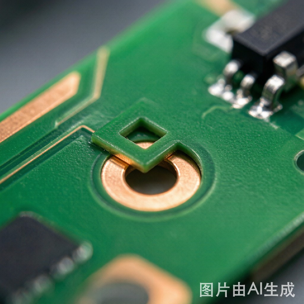
## Solder Mask: The Unsung Hero of SMT Assembly Yield
Solder mask—the thin polymer coating applied over PCB copper traces—serves a deceptively simple purpose: prevent solder from wetting where it should not. Yet this seemingly modest function directly determines SMT assembly yield for fine-pitch components. When solder mask clearance and registration are correctly designed, the mask creates precise dams between adjacent pads, preventing solder bridging during reflow. When clearance or registration errs, the mask either encroaches onto pads (causing solder opens and insufficient fillet formation) or fails to separate pads (allowing bridges between 0.4 mm pitch QFP leads or 0.5 mm pitch BGA balls).
For copper-rich PCBs common in power electronics, LED lighting, and automotive applications, solder mask design rules become even more critical because the copper thickness affects mask adhesion, planarity, and registration accuracy. A solder mask misregistration of 50 μm that is barely noticeable on a 1 oz copper board with generous pad spacing becomes a catastrophic defect when it exposes adjacent 4 oz copper pours or bridges 0.3 mm wide mask dams.
## Solder Mask Clearance: The Critical Dimension
### What is Solder Mask Clearance?
Solder mask clearance (also called solder mask expansion or solder mask swell) is the a
ular ring around a copper pad where the solder mask does NOT cover. This opening exposes the copper pad for soldering while the mask covers the surrounding copper traces. The clearance dimension is measured from the edge of the copper pad to the edge of the solder mask opening.
The clearance value represents a deliberate design compromise:
– Too small (or negative): Solder mask encroaches onto the pad, reducing wettable pad area and potentially covering the pad edge where solder fillets should form
– Too large: Exposes adjacent copper that should be masked, increasing bridging risk and potentially exposing via a
ular rings or adjacent traces
### IPC-7351 and IPC-SM-840 Design Rules
IPC standards provide baseline solder mask clearance recommendations:
| Pad Type | IPC Recommended Clearance | Practical Range |
|—|—|—|
| Standard SMT (≥1.0 mm pitch) | 50-75 μm (2-3 mil) | 50-100 μm |
| Fine-pitch (0.5-0.8 mm) | 25-50 μm (1-2 mil) | 25-75 μm |
| Ultra-fine-pitch (≤0.4 mm) | 15-25 μm (0.5-1 mil) | 15-50 μm |
| BGA pads | 50-75 μm | 50-100 μm |
| QFN thermal pad (segmented) | 50-100 μm | 50-150 μm |
These recommended clearances assume a PCB fabrication capability of ±50 μm (2 mil) registration tolerance. When using a fabricator with tighter registration (±25 μm or better), clearances can be reduced proportionally.
### The Solder Mask Dam: Preventing Bridges
Between adjacent pads, the solder mask forms a narrow ridge called a “solder mask dam” that physically separates the two pads. The dam width is the most critical dimension for fine-pitch bridging prevention:
Dam width = (Pad pitch) – (Pad width) – (2 × Solder mask clearance)
For a 0.5 mm pitch QFP:
– Pad width: 0.25 mm
– Solder mask clearance: 0.05 mm (each side)
– Dam width = 0.50 – 0.25 – (2 × 0.05) = 0.15 mm
This 0.15 mm (6 mil) dam is the physical barrier preventing a solder bridge. If registration shifts by 50 μm (2 mil), one side of the dam reduces to 0.10 mm (4 mil) while the other side opens to 0.20 mm—still functional but with reduced margin.
### Minimum Dam Width by Technology
| Technology | Pitch | Pad Width | Min Clearance | Calculated Dam | Viable? |
|—|—|—|—|—|—|
| Standard QFP | 0.8 mm | 0.40 mm | 0.075 mm | 0.25 mm (10 mil) | Yes, robust |
| Fine-pitch QFP | 0.5 mm | 0.25 mm | 0.050 mm | 0.15 mm (6 mil) | Yes, with ±50 μm registration |
| Ultra-fine QFP | 0.4 mm | 0.20 mm | 0.040 mm | 0.12 mm (4.7 mil) | Marginal—requires ±35 μm registration |
| BGA (1.0 mm) | 1.0 mm | 0.50 mm | 0.075 mm | 0.35 mm (14 mil) | Yes, very robust |
| BGA (0.8 mm) | 0.8 mm | 0.40 mm | 0.075 mm | 0.25 mm (10 mil) | Yes, robust |
| BGA (0.5 mm) | 0.5 mm | 0.28 mm | 0.050 mm | 0.12 mm (4.7 mil) | Marginal |
| 0201 chip | 0.60 mm | 0.30 mm | 0.050 mm | 0.20 mm (8 mil) | Yes |
| 01005 chip | 0.40 mm | 0.20 mm | 0.040 mm | 0.12 mm (4.7 mil) | Marginal |
The 0.12 mm (4.7 mil) dam width represents the practical minimum for most PCB fabricators. Below this, registration tolerances consume the entire dam margin, and bridging risk increases sharply.
## Solder Mask Registration: The Tolerance Budget
### Sources of Registration Error
Solder mask registration is the alignment accuracy between the solder mask opening and the copper pad. The total registration error is the vector sum of multiple independent error sources:
1. Copper pattern registration (±25-75 μm): The etched copper pad position relative to the design position, determined by photolithography alignment accuracy
2. Solder mask artwork alignment (±25-50 μm): The mask photo-tool alignment to the copper pattern
3. Solder mask imaging resolution (±15-25 μm): The minimum feature size the mask photo-process can resolve
4. Solder mask development undercut (±10-25 μm): Lateral etching of mask during development, enlarging openings beyond design
5. Copper thickness variation (±10-20 μm): Thicker copper creates taller pad edges that affect mask coating thickness and resolution
The root-sum-square (RSS) total registration error for a typical fabricator:
RSS = √(50² + 35² + 20² + 15² + 15²) = √(2500 + 1225 + 400 + 225 + 225) = √4575 ≈ 68 μm
A fabricator with ±68 μm (2.7 mil) registration tolerance requires solder mask clearance of at least 50-75 μm per side to prevent pad encroachment. Advanced fabricators achieve ±35 μm total error through tighter process control, enabling finer clearances.
### Registration Defect Mechanisms
Two types of registration defects affect SMT assembly yield:
Type 1: Mask-on-Pad (Negative Registration Error)
The mask opening shifts relative to the copper pad so that mask material covers part of the pad. Consequences:
– Reduced wettable pad area—smaller solder fillet, reduced mechanical strength
– Mask covering the pad edge prevents fillet formation at the pad toe (where most stress concentrates)
– For fine-pitch pads, even 25-50 μm of pad coverage reduces the exposed pad width by 10-20%, significantly reducing solder joint reliability
Type 2: Mask-off-Pad (Positive Registration Error)
The mask opening shifts away from the pad, exposing adjacent copper that should be masked. Consequences:
– Exposed adjacent traces create unintended solder wetting surfaces—bridges form between pads
– Exposed via pads near SMT pads wick solder away from the component pad during reflow (solder wicking/solder thief effect)
– Lateral mask opening exposes copper under the mask edge, creating potential solder balls at the mask-copper interface
### Registration Budget Example: 0.5 mm QFP
For a 0.5 mm pitch QFP with 0.25 mm pad width, using ±68 μm registration tolerance:
| Parameter | Value |
|—|—|
| Pad width | 0.25 mm |
| Nominal clearance each side | 0.050 mm |
| Nominal mask opening width | 0.35 mm (0.25 + 2×0.05) |
| Registration error (worst case) | 0.068 mm |
| Mask opening at worst negative registration | 0.282 mm (0.35 – 0.068) |
| Remaining exposed pad width | 0.25 mm (mask opening still exceeds pad width) |
| Pad coverage at worst negative | 0 mm (just at edge—no coverage) |
| Dam width at worst negative (other side) | 0.218 mm (widened) |
| Dam width at worst positive (this side) | 0.082 mm (dangerously narrow) |
This analysis reveals that even with the nominally acceptable IPC-minimum 50 μm clearance, the dam width on one side drops to 82 μm under worst-case registration—leaving only 14 μm of margin above the practical minimum after accounting for the 68 μm registration error. A 100 μm (4 mil) clearance provides significantly better margin.
## Copper Thickness Effects on Solder Mask Design
### Heavy Copper Mask Challenges
Heavy copper boards (3 oz and above) present unique solder mask challenges:
– Copper step height: 3 oz copper thickness = 105 μm, creating a vertical step between the pad surface and the laminate surface that the mask must cover. Liquid photoimageable (LPI) solder mask flows over this step, thi
ing at the step edge—the thi
est mask coverage point.
– Mask adhesion: Thick copper edges with vertical sidewalls challenge mask adhesion—the mask must wrap over the copper edge and adhere to both the copper top surface and the laminate between traces.
– Registration accuracy: Taller copper features create shadowing during mask imaging exposure, affecting edge definition and registration accuracy near copper features.
### Design Rules for Heavy Copper
| Copper Weight | Min Clearance | Min Dam Width | Notes |
|—|—|—|—|
| 1 oz (35 μm) | 50 μm | 100 μm (4 mil) | Standard rules apply |
| 2 oz (70 μm) | 75 μm | 125 μm (5 mil) | Moderate step height |
| 3 oz (105 μm) | 100 μm | 150 μm (6 mil) | Significant step height |
| 4 oz (140 μm) | 125 μm | 175 μm (7 mil) | Two mask coats may be required |
| 6 oz (210 μm) | 150 μm | 200 μm (8 mil) | Two mask coats essential |
| 10 oz (350 μm) | 200 μm | 250 μm (10 mil) | Special process; consult fabricator |
For 4 oz and heavier copper, applying two solder mask coats improves coverage at copper edges—the first coat fills the copper-laminate step, and the second coat provides uniform top-surface coverage.
## Practical Design Guidelines
### Clearance Selection by Application Risk
| Risk Level | Application | Recommended Clearance |
|—|—|—|
| Low (consumer, 1-2 oz, ≥0.8 mm pitch) | Standard consumer electronics | 50-75 μm |
| Medium (industrial, 2-3 oz, ≥0.5 mm pitch) | Industrial controls, LED lighting | 75-100 μm |
| High (automotive, 3-4 oz, ≥0.5 mm pitch) | Automotive ECUs, power modules | 100-125 μm |
| Critical (aerospace/medical, mixed copper, ≤0.5 mm pitch) | Avionics, implantable medical | 125-150 μm + fabricator capability review |
### Verification Checklist Before PCB Release
1. Verify minimum dam width ≥ 100 μm (4 mil) for standard technology, ≥ 125 μm (5 mil) for heavy copper
2. Check that clearance + registration tolerance < pad-to-adjacent-copper distance—a 125 μm clearance + 75 μm registration error must not expose adjacent copper
3. Review solder mask openings at via pads near SMT pads—unmasked vias act as solder thieves
4. Confirm mask opening dimensions match the fabricator's minimum LPI resolution (typically 75-100 μm)
5. For mixed copper weight boards, use the heavier copper's clearance rules globally (a 4 oz zone's rules apply to adjacent 1 oz zones on the same board)
## Conclusion: Clearance and Registration as Yield Determinants
Solder mask clearance and registration tolerance are not aesthetic PCB design choices—they are manufacturing yield and reliability determinants. A correctly designed solder mask, with adequate clearance for the PCB fabricator's registration capability and proper dam width for the component pitch, prevents both solder bridging and insufficient fillet formation. An incorrectly designed mask, with clearance that assumes zero registration error or dam width that assumes perfect alignment, produces assembly defects that are difficult to diagnose because they appear as process problems rather than design problems.
For fine-pitch SMT assembly on copper-rich PCBs—increasingly common in power electronics, automotive, and industrial applications—investing the design effort to calculate solder mask tolerances and verify minimum dam widths against the fabricator's published capability prevents field failures that cost far more than the design time required.



