## EMI Shielding Can Attachment: A Critical Design Decision
Electromagnetic interference (EMI) shielding cans—those metal covers mounted over sensitive circuit areas on PCBs—must attach to the board in a way that maintains continuous electrical contact across the entire can perimeter. The attachment method determines three critical outcomes: shielding effectiveness (how many dB of EMI attenuation the can provides), manufacturing cost (labor, equipment, and throughput implications), and rework capability (whether the can can be removed and replaced without damaging the PCB).
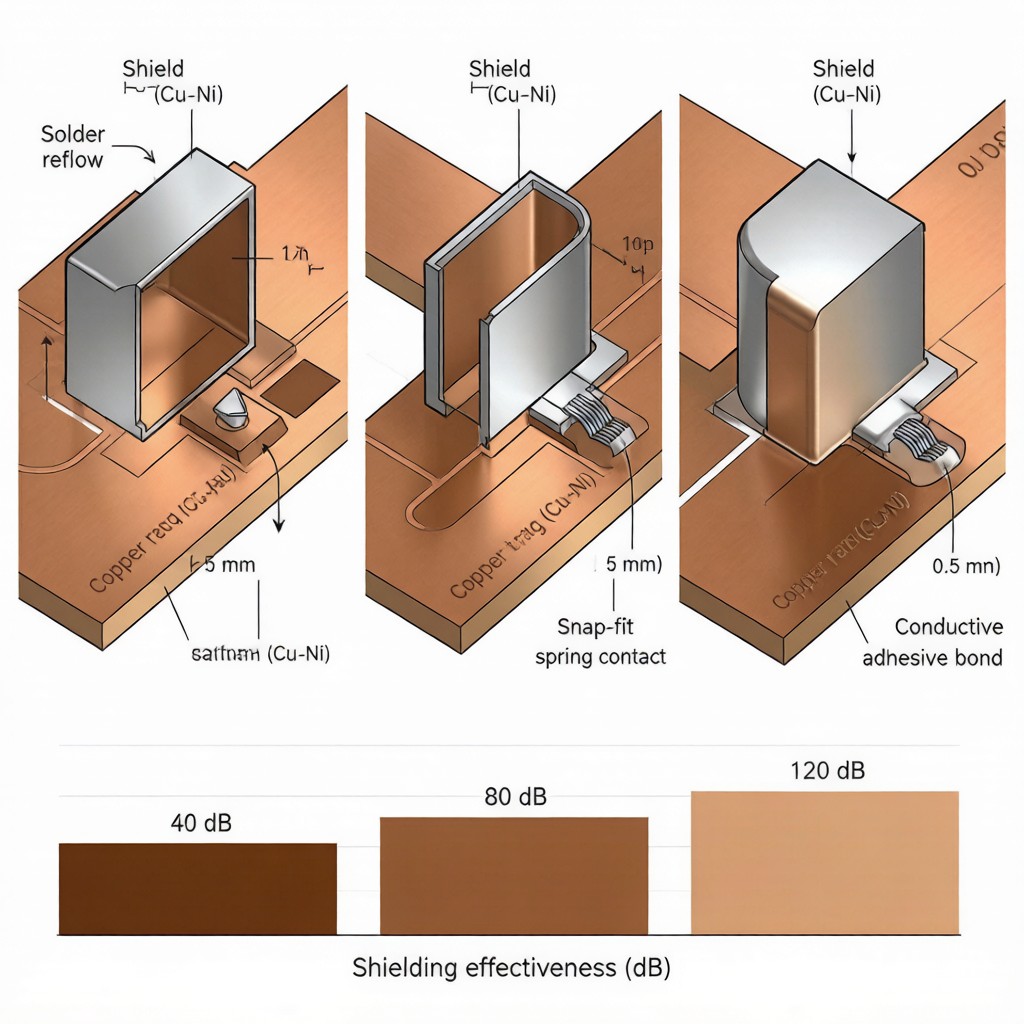
Three attachment methods dominate current SMT electronics manufacturing: solder reflow attachment, snap-fit clip attachment, and conductive adhesive bonding. Each method offers distinct advantages and limitations that make it optimal for specific application scenarios. This article provides a quantitative comparison of all three methods to guide your EMI shielding can design decisions.
## Solder Reflow Attachment: The Traditional Standard
### How Solder Attachment Works
Solder reflow attachment mounts the shielding can during the standard SMT reflow process. The can’s mounting flange sits on solder paste deposits printed on a perimeter pad pattern around the shielded area. During reflow, the solder melts and forms fillets co
ecting the can flange to the PCB pad, creating both mechanical fixation and electrical continuity.
This method integrates seamlessly into existing SMT production flows—no additional equipment, no secondary operations, no extra process steps. The shielding can is placed by the same pick-and-place machine that deposits other SMT components, and reflowed in the same oven pass.
### Solder Attachment Performance
| Parameter | Typical Value | Notes |
|—|—|—|
| Shielding effectiveness | 80-120 dB (DC-LF) | Excellent—continuous metal-to-metal solder joint perimeter |
| SE at 1 GHz | 70-100 dB | Solder joint impedance rises at RF frequencies |
| SE at 5 GHz | 50-80 dB | Joint inductance creates RF leakage paths |
| Mechanical strength | 15-25 N/cm | Strong—solder fillet provides robust mechanical bond |
| Rework capability | Difficult | Hot air rework required; risk of pad lifting on 2+ layer boards |
| Assembly cost | Lowest | No additional process steps beyond standard SMT reflow |
### Solder Attachment Limitations
Despite its simplicity and effectiveness, solder attachment has notable limitations:
– Thermal stress on shielded components: The entire board passes through reflow oven (peak 250°C for SAC305), exposing shielded components to full thermal profile—problematic for temperature-sensitive devices
– One-time attachment: Solder joints are permanent; removal requires localized heating that risks damaging adjacent components and PCB pads
– Solder joint gap formation: If the can flange is not perfectly coplanar with the PCB surface, gaps in the solder perimeter create EMI leakage slots—even a 0.1 mm gap can reduce SE by 20-30 dB at GHz frequencies
– Voiding: Solder voids under the can flange (similar to QFN/BGA voiding) create localized SE degradation and mechanical weakness
## Snap-Fit Clip Attachment: Post-Reflow Flexibility
### How Snap-Fit Attachment Works
Snap-fit shielding cans use spring clips integrated into the can’s mounting flange that engage with corresponding slots or posts on the PCB. The can is installed after SMT reflow—pressing the can onto the board causes the clips to snap into the PCB features, creating both mechanical retention and electrical contact through spring force.
The PCB features that receive snap-fit clips can be either:
– Plated through-holes (via-like slots) that the clips insert into, providing vertical retention and side-wall contact
– Surface pads with clip retention features that the clips grip horizontally
Both approaches create electrical contact through the spring force of the clip engaging against copper or plated surfaces.
### Snap-Fit Attachment Performance
| Parameter | Typical Value | Notes |
|—|—|—|
| Shielding effectiveness | 40-80 dB (DC-LF) | Good but lower than solder—spring contact resistance creates perimeter impedance |
| SE at 1 GHz | 30-60 dB | Clip contact impedance limits RF shielding |
| SE at 5 GHz | 20-40 dB | Spring clip inductance dominates at microwave frequencies |
| Mechanical strength | 5-10 N/cm | Moderate—retention depends on clip spring force |
| Rework capability | Excellent | Can removed and replaced without heating; clips re-engage reliably |
| Assembly cost | Medium | Requires post-reflow manual or automated can installation |
### Snap-Fit Advantages for Specific Applications
Snap-fit attachment excels in scenarios where solder reflow is problematic:
– Post-reflow installation: Shielding can placed after reflow avoids thermal exposure of sensitive shielded components (RFICs, MEMS sensors, crystal oscillators)
– Prototype and development: Easy removal enables access to shielded circuitry for debugging, measurement, and modification
– Field service: Repair technicians can remove and replace cans without soldering equipment
– Multi-cavity shields: Large cans covering multiple circuit blocks can incorporate removable sub-covers for selective access
### Snap-Fit Limitations
The primary limitations of snap-fit attachment are shielding effectiveness and long-term reliability:
– Contact resistance variability: Spring clip contact force varies with PCB surface finish, plating quality, and dimensional tolerances—creating non-uniform perimeter impedance
– Aging degradation: Clip spring force relaxes over time (especially at elevated operating temperatures), reducing both mechanical retention and electrical contact quality
– Vibration sensitivity: Under mechanical vibration, clip contacts can momentarily separate, creating transient EMI leakage events
– Limited RF performance: Spring clip inductance at GHz frequencies creates perimeter impedance that limits SE to 20-40 dB at 5 GHz—insufficient for many RF/microwave applications
## Conductive Adhesive Attachment: The Emerging Option
### How Conductive Adhesive Works
Conductive adhesive (also called electrically conductive adhesive, ECA) bonds the shielding can to the PCB using an adhesive compound loaded with conductive particles—typically silver flakes (60-80% loading by weight) in an epoxy or silicone matrix. The adhesive is dispensed as a perimeter bead around the shielded area, the can is placed onto the bead, and the adhesive cures through thermal or UV activation.
Silver-loaded epoxy adhesive provides electrical conductivity through percolation pathways between overlapping silver flakes, achieving bulk conductivity of 10⁻³-10⁻² S/cm depending on loading fraction and flake geometry.
### Conductive Adhesive Performance
| Parameter | Typical Value | Notes |
|—|—|—|
| Shielding effectiveness | 60-100 dB (DC-LF) | Good—continuous adhesive bead provides uniform perimeter contact |
| SE at 1 GHz | 40-70 dB | Adhesive bulk impedance rises at RF |
| SE at 5 GHz | 20-50 dB | Particle-to-particle contact impedance dominates |
| Mechanical strength | 8-15 N/cm | Moderate—adhesive bond strength depends on cure quality |
| Rework capability | Moderate | Adhesive softens at 80-120°C; removal possible but leaves residue |
| Assembly cost | Medium-High | Requires adhesive dispensing equipment + cure step |
### Conductive Adhesive Advantages
Conductive adhesive offers unique benefits for specific manufacturing scenarios:
– Low-temperature assembly: Cure temperatures of 80-120°C (vs 250°C for solder reflow) avoid thermal stress on temperature-sensitive components
– Flexible substrate compatibility: Adhesive bonding works on flexible PCBs and irregular surfaces where solder wetting is unreliable
– Gap compensation: Adhesive bead thickness (0.1-0.3 mm) accommodates surface non-planarity that would create gaps in solder joints
– Mixed-material bonding: Silver epoxy bonds copper cans to aluminum, nickel, or stainless steel PCB features without the intermetallic compatibility concerns of solder
### Conductive Adhesive Limitations
Current conductive adhesive technology has important limitations:
– Cure time: Thermal cure requires 30-60 minutes at elevated temperature; UV cure is faster (5-10 minutes) but requires UV-transparent can designs or dispensing access
– Cost: Silver-loaded adhesive costs 5-10x more than solder paste per perimeter length, making it expensive for large cans
– Long-term stability: Silver flake contact resistance increases 10-30% over 1000 hours at 85°C operating temperature (contact oxidation between flakes)
– Moisture sensitivity: Some epoxy-based adhesives absorb moisture, increasing bulk resistance in high-humidity environments common in Southeast Asia
## Comprehensive Comparison: Choosing the Right Method
### Quantitative SE Comparison Across Frequency Ranges
| Frequency | Solder Reflow | Snap-Fit Clip | Conductive Adhesive | Critical Application |
|—|—|—|—|—|
| DC-10 MHz | 100-120 dB | 50-80 dB | 80-100 dB | Power supply noise shielding |
| 10-100 MHz | 80-100 dB | 40-60 dB | 60-80 dB | MCU clock harmonics |
| 100-1000 MHz | 70-90 dB | 30-50 dB | 40-70 dB | WiFi/BT/LTE shielding |
| 1-5 GHz | 50-80 dB | 20-40 dB | 20-50 dB | 5G/mmWave shielding |
| >5 GHz | 40-60 dB | 15-25 dB | 15-35 dB | Radar/satellite |
### Decision Matrix by Application Priority
| Priority | Recommended Method | Reason |
|—|—|—|
| Maximum SE (DC-1 GHz) | Solder reflow | Continuous perimeter joint provides highest SE |
| Post-reflow installation | Snap-fit or adhesive | Avoid thermal exposure of shielded components |
| Rework / service access | Snap-fit | Easy removal without heating |
| Cost minimization | Solder reflow | No additional process steps |
| Temperature-sensitive components | Snap-fit or adhesive | Low or no thermal exposure |
| 5G/mmWave SE >40 dB | Solder (only viable option) | Snap-fit and adhesive insufficient at GHz |
| Flexible PCB | Conductive adhesive | Solder unreliable on flex; snap-fit needs rigid features |
## Southeast Asia Manufacturing Considerations
For SMT electronics manufacturing in Southeast Asia, several regional factors influence attachment method selection:
– High humidity accelerates conductive adhesive resistance degradation—silver epoxy should specify moisture-resistant formulations for SE Asia deployment
– Cost sensitivity in high-volume consumer electronics favors solder reflow attachment for its zero-additional-cost integration into standard SMT process
– Rework requirements for automotive and industrial electronics favor snap-fit for field service accessibility
– Emerging 5G device production requires solder attachment as the only method achieving >40 dB SE at mmWave frequencies
## Conclusion: Method Selection as an Integrated Design Decision
EMI shielding can attachment method selection ca
ot be made in isolation—it depends on the required shielding frequency range, manufacturing process flow, rework needs, and cost constraints specific to each application. Solder reflow remains the performance leader for SE across all frequencies and the cost leader for standard SMT production. Snap-fit offers unmatched rework flexibility and post-reflow installation at moderate SE levels. Conductive adhesive bridges the gap with low-temperature bonding and gap-compensation capability, but at higher material cost and with long-term stability considerations.
Choose the method that satisfies your most critical requirement first (SE at your target frequency, rework access, or cost), then verify that secondary requirements fall within that method’s capability range. For applications where no single method satisfies all requirements, hybrid approaches—solder on high-SE critical edges with snap-fit on service-access edges—can optimize across multiple constraints simultaneously.



