The Hidden Soldering Challenge: PCB Pad Co
ection Design
Every SMT component sits on a copper pad that co
ects to the broader circuit—traces, ground planes, or power pours. How that pad co
ects to surrounding copper determines whether solder flows properly during reflow or gets starved by the thermal mass of an attached plane. This seemingly minor PCB design decision—thermal relief pad versus direct copper co
ect—has profound impact on solder joint quality, especially on high-copper-weight boards with heavy ground and power planes.
The problem is simple physics: solder reflow requires each pad to reach liquidus temperature (217°C for SAC305) and maintain sufficient time-above-liquidus for proper wetting. A pad directly co
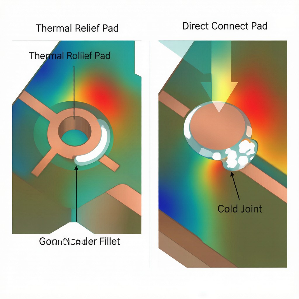
ected to a large copper plane acts as a thermal conduit, draining heat from the pad into the plane and creating a localized cold spot. A thermal relief pad, co
ected through narrow spokes, limits this heat drain and allows the pad to reach proper reflow temperature alongside isolated pads.
Yet the choice between thermal relief and direct co
ect involves trade-offs that extend beyond soldering thermal dynamics. Current-carrying capacity, impedance continuity, and electromagnetic compatibility all factor into the decision. Understanding these trade-offs enables PCB designers to make informed pad co
ection choices that optimize both manufacturing yield and circuit performance.
## Thermal Relief Pad Design: Structure and Function
### The 4-Spoke Thermal Relief Pattern
A thermal relief pad (also called a “thermals” or “flash” pad) co
ects to the copper plane through 2-4 narrow spoke traces, typically 0.2-0.4 mm (8-16 mil) wide, with an air gap between the pad and the surrounding pour. The standard configuration uses 4 spokes at 90° intervals, though 2-spoke designs appear on narrow pads where 4 spokes would consume excessive pad area.
The spokes serve two functions simultaneously:
1. Thermal resistance: By restricting the copper cross-section between pad and plane, spokes increase thermal resistance from approximately 1-5°C/W (direct co
ect) to 15-40°C/W (thermal relief), allowing the pad to heat independently during reflow
2. Electrical continuity: The spokes maintain a DC current path from pad to plane, though with higher resistance than a direct pour co
ection
### Spoke Width and Air Gap Parameters
| Parameter | Typical Range | Effect on Soldering | Effect on Current |
|—|—|—|—|
| Spoke width | 8-16 mil (0.2-0.4 mm) | Narrower spokes = better thermal isolation | Narrower spokes = higher DC resistance |
| Air gap width | 8-20 mil (0.2-0.5 mm) | Wider gap = better thermal isolation | Wider gap = no current effect |
| Number of spokes | 2-4 (standard: 4) | More spokes = less isolation benefit | More spokes = lower total resistance |
| Spoke angle | 45° or 90° intervals | No thermal effect | 45° can fit on smaller pads |
The thermal isolation effect scales with spoke width. For a ground plane on 2 oz (70 μm) copper, 4 spokes at 10 mil width provide approximately 25°C/W thermal resistance—sufficient for most SMT reflow applications. On 4 oz (140 μm) copper, the same spoke geometry provides only 12-15°C/W, and wider spokes or fewer spokes may be needed for adequate isolation.
## Direct Co
ect Pads: Full Copper Pour Contact
### Structure and Thermal Behavior
A direct co
ect pad merges seamlessly into the surrounding copper pour with no spokes or air gaps. The pad and plane are a single conductive region. This provides:
– Minimum thermal resistance: 1-5°C/W between pad and plane, depending on copper weight and plane area
– Minimum DC resistance: Essentially zero additional resistance beyond the plane’s bulk conductivity
– Maximum current capacity: Full plane cross-section available for current delivery
– Continuous impedance: No discontinuity in ground or power plane impedance at the pad location
### The Soldering Problem with Direct Co
ects
During reflow, the direct co
ect pad experiences a severe thermal disadvantage compared to isolated pads on the same board. The copper plane acts as an infinite heat sink—energy applied to the pad by the reflow oven conducts into the plane rather than heating the pad to liquidus temperature. This manifests as:
1. Delayed wetting: The pad reaches liquidus 10-30 seconds after adjacent isolated pads, producing uneven wetting across the board
2. Reduced wetting spread: Solder that does melt on the pad has less time-above-liquidus, resulting in smaller wetting area and thi
er fillets
3. Cold solder joints: On heavy copper (3 oz+), direct co
ect pads may never reach sufficient temperature, producing gray, grainy joints that fail IPC-A-610 Class 2 criteria
4. Tombstoning differential: Components straddling a direct-co
ect pad and an isolated pad experience asymmetric heating, creating the thermal gradient that drives tombstoning (one end wets, the other doesn’t)
## Quantifying the Thermal Impact
### Temperature Differential During Reflow
Thermal simulation data from SMTA conference papers demonstrates the temperature gap between thermal relief and direct co
ect pads on a 2 oz copper board during typical SAC305 reflow (peak 250°C):
| Pad Type | Time to Liquidus (217°C) | Peak Temperature | Time Above Liquidus | Wetting Spread Ratio |
|—|—|—|—|—|
| Isolated pad (no plane) | 45 s | 248°C | 65 s | 1.00 (reference) |
| Thermal relief (4×10 mil spokes, 2 oz) | 50 s | 244°C | 55 s | 0.88 |
| Thermal relief (4×10 mil spokes, 4 oz) | 58 s | 238°C | 40 s | 0.72 |
| Direct co
ect (2 oz plane) | 65 s | 230°C | 25 s | 0.55 |
| Direct co
ect (4 oz plane) | 75 s | 222°C | 8 s | 0.35 |
The data reveals that direct co
ect pads on 4 oz copper reach only marginally above liquidus—just 5°C and 8 seconds of time-above-liquidus. This is insufficient for SAC305 wetting, which requires minimum 30 seconds above 217°C per IPC-J-STD-006 recommendations.
### When Direct Co
ects Cause Production Defects
On heavy copper boards (3 oz and above), direct co
ect pads on ground/power planes produce a characteristic defect profile:
– **20-35% of direct-co
ect pads** show incomplete wetting on 3 oz copper boards
– **50-70% of direct-co
ect pads** fail wetting on 4 oz+ copper boards
– Tombstoning rate for components bridging direct-co
ect and isolated pads increases 5-8x compared to uniform thermal relief designs
– Rework rate for direct-co
ect pad joints runs 3-5x higher than thermal relief pads on the same board
These statistics justify thermal relief as the default design choice for all pads co
ecting to planes on boards with 2 oz or heavier copper.
## Design Decision Framework: When to Use Each Approach
### Always Use Thermal Relief
– Ground and power plane pads on 2 oz or heavier copper boards
– Via pads on heavy copper planes (via barrels also co
ect to the plane, compounding heat sink effect)
– Component pads near plane edges where the plane extends far in one direction
– BGA pads on power/ground balls—uneven thermal profile causes BGA warpage
### Consider Direct Co
ect
– 1 oz copper boards where thermal mass is small enough that reflow oven energy overcomes the heat sink effect
– High-current pads (>2A continuous) where spoke resistance creates unacceptable voltage drop or thermal rise under load
– RF/microwave pads where impedance discontinuity at spokes creates signal integrity degradation
– High-frequency ground pads where spoke inductance compromises return path continuity above 1 GHz
### Hybrid Approaches
Some designs require hybrid pad co
ection strategies:
– Wider spokes (20-25 mil) on power delivery pads that need both soldering reliability and current capacity—wider spokes reduce thermal isolation somewhat but improve current handling
– **Selective direct co
ect** on non-soldered mechanical pads (mounting holes, test points) where soldering is not required but current continuity is
– Partial relief with 2 spokes instead of 4 on pads where moderate thermal isolation suffices and current capacity needs only 2 conductive paths
## Impact on Southeast Asia SMT Manufacturing
### Humidity and Reflow Profile Considerations
Southeast Asia manufacturing environments present additional challenges for thermal relief vs direct co
ect decisions:
– High ambient humidity (70-85% RH) increases PCB moisture absorption, which can cause delamination during reflow—thermal relief pads reduce localized thermal stress, lowering delamination risk on heavy copper boards
– Shorter reflow profiles preferred in high-volume SE Asia factories reduce time-above-liquidus, making thermal isolation more critical for achieving adequate wetting
– Mixed-technology boards (SMT + through-hole) common in SE Asia automotive electronics require careful pad design to accommodate both wave soldering and reflow soldering thermal requirements
### Design Review Checklist
Before releasing PCB designs for SMT manufacturing in Southeast Asia:
1. Verify all ground/power plane pads use thermal relief on 2 oz+ copper
2. Confirm spoke width ≥10 mil on 2-3 oz copper, ≥15 mil on 4 oz+ (wider for better current)
3. Check that high-current pads have calculated voltage drop through spokes (<50 mV for most applications)
4. Ensure BGA ground/power pads use thermal relief to prevent warpage-induced open circuits
5. Review reflow profile with thermal simulation to verify all pad types reach minimum time-above-liquidus
## Conclusion: Pad Design as a Manufacturing Yield Driver
The choice between thermal relief pad and direct co
ect is not a minor layout preference—it is a manufacturing yield decision that directly affects solder joint quality, defect rates, and rework costs. Thermal relief pads should be the default choice for all plane-co
ected pads on 2 oz and heavier copper boards, with direct co
ect reserved for applications where spoke resistance or impedance discontinuity creates verified circuit performance problems.
For SMT manufacturers in Southeast Asia producing heavy copper boards for automotive, industrial, and power electronics applications, proper thermal relief design is one of the most cost-effective yield improvements available—requiring only design rule discipline, no additional process investment, and delivering immediate defect reduction on the production floor.



