At frequencies above 1 GHz, the surface properties of an EMI shielding component — not its bulk material — determine shielding effectiveness. The phenomenon driving this is the skin effect: alternating current concentrates in a thin layer at the conductor surface, and the depth of this layer (the skin depth) shrinks as frequency increases. For copper at 1 GHz, the skin depth is 2.1 μm. At 10 GHz, it is 0.66 μm. At 30 GHz (mmWave 5G), it is 0.38 μm. The plating on a copper EMI shielding component — whether silver, nickel, or something else — is often thicker than the skin depth, meaning the plating material, not the copper substrate, carries the majority of the RF current. This makes plating selection a first-order RF design decision, not a cosmetic afterthought.
Skin Effect and Its Impact on EMI Shielding
The skin depth δ (in meters) for a non-magnetic conductor at frequency f (Hz) is:
δ = √(ρ / (π · f · μ₀))
Where ρ is the electrical resistivity (Ω·m) and μ₀ = 4π × 10⁻⁷ H/m. For a given frequency, lower resistivity produces shallower skin depth — counterintuitively, because lower resistivity also produces lower resistance per unit skin depth. The relevant figure of merit for shielding is the surface resistivity Rₛ = ρ/δ, with units Ω/square. Lower surface resistivity means better shielding.
| Material | Resistivity (μΩ·cm) | Relative Permeability | Skin Depth at 1 GHz | Surface Resistivity at 1 GHz (mΩ/sq) |
|---|---|---|---|---|
| Silver (pure) | 1.59 | 1 | 2.0 μm | 7.9 |
| Copper (pure) | 1.72 | 1 | 2.1 μm | 8.2 |
| Silver (electroplated, bright) | 1.8–2.2 | 1 | 2.1–2.4 μm | 8.6–9.3 |
| Nickel (electroplated, sulfamate) | 7.8–10 | 1 | 4.4–5.0 μm | 17–20 |
| Nickel (electroless, mid-phos) | 55–90 | 1 | 12–15 μm | 46–60 |
| Nickel (Watts, bright) | 9–14 | 1 | 4.8–6.0 μm | 19–23 |
The surface resistivity of electroplated silver (8.6–9.3 mΩ/sq at 1 GHz) is approximately half that of nickel (17–23 mΩ/sq). This translates directly to shielding effectiveness: a silver-plated copper shield has approximately 6 dB better shielding effectiveness than a nickel-plated copper shield of identical geometry, due solely to the lower surface resistivity. This 6 dB difference can be the margin between passing and failing regulatory EMC compliance.
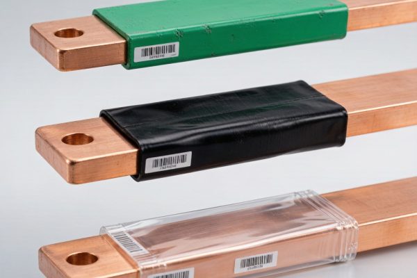
Silver Plating for RF Shielding
Silver electroplating on copper EMI shielding components provides the best possible surface conductivity — approaching that of pure silver — because silver has the lowest electrical resistivity of any metal (1.59 μΩ·cm for pure silver, 1.8–2.2 μΩ·cm for electroplated bright silver). For high-frequency applications, this translates to:
- Lower insertion loss: Silver-plated RF co
ectors, waveguide flanges, and shield joints exhibit lower insertion loss than nickel-plated equivalents. For a typical SMA co
ector at 18 GHz, silver plating reduces insertion loss by 0.05–0.10 dB compared to nickel — a small number per co
ector, but significant in systems with 20+ co
ector pairs.
- Higher shielding effectiveness: The 2× lower surface resistivity translates to approximately 6 dB higher SE for thin shields (where absorption loss, not reflection loss, dominates). This is most significant above 5 GHz where skin depth is shallow enough that the nickel layer’s higher resistivity limits shielding performance.
- Lower passive intermodulation (PIM): Silver-to-silver contacts produce lower PIM than nickel-to-nickel or nickel-to-silver contacts. For cellular base station and satellite applications, PIM specifications of < -160 dBc are common; silver plating is one of the few surface finishes that can consistently meet this requirement.
Silver plating challenges: Silver tarnishes in ambient air. Silver sulfide (Ag₂S) forms a dark, non-conductive layer that increases contact resistance and degrades RF performance over time. For indoor, climate-controlled environments (< 50% RH, low sulfur), silver tarnish is manageable with anti-tarnish post-treatments (benzotriazole-based immersion, or proprietary organic coatings). For outdoor or industrial environments with H₂S or SO₂ exposure, silver requires a protective overplate — typically 0.1–0.5 μm of gold, or a thin organic coating — that maintains surface conductivity while preventing tarnish. This adds cost, making silver plating a premium option.
Silver migration is another concern for DC-biased circuits with closely spaced silver-plated conductors. Under high humidity (> 85% RH) and DC bias, silver ions migrate across insulating surfaces, forming conductive dendrites that create short circuits. For EMI shielding applications, this is typically not a concern because shield surfaces are not DC-biased, but it is a consideration for combined shield/signal applications.
Nickel Plating for RF Shielding
Nickel plating is the workhorse surface finish for EMI shielding components, and for many applications, its RF performance is adequate. The advantages of nickel:
- Corrosion resistance: Nickel forms a stable, self-limiting oxide (NiO) that protects the underlying copper from corrosion in most environments. No tarnish issue comparable to silver. Nickel-plated copper shields can operate in 85°C/85% RH environments for 1,000+ hours without significant degradation.
- Wear resistance: Nickel (150–400 HV) is significantly harder than silver (60–100 HV), providing better wear durability for co
ector shells, spring contacts, and mating surfaces. For EMI gasket applications with 100,000+ insertion cycles, nickel’s wear resistance is a major advantage.
- Lower cost: Nickel plating chemistry costs $3–12/kg versus $200–400/kg for silver plating chemistry (silver cyanide or silver methanesulfonate). The material cost of a 2.5 μm nickel plate is approximately $0.01–0.03/m²; silver plate of the same thickness is $0.50–1.50/m².
- Solderability: Nickel surfaces are solderable with RMA or water-soluble flux, though they require more active flux than silver or gold surfaces. Electroless nickel immersion gold (ENIG) combines nickel’s corrosion protection with a thin gold layer for superior solderability, but ENIG on copper strip is expensive and primarily used for PCB pads, not stamped EMI components.
Nickel plating limitations for RF: Nickel is ferromagnetic (though electrolytic nickel has relative permeability ~1, some nickel deposits have slightly elevated permeability that increases magnetic losses). The higher resistivity of nickel (7.8–10 μΩ·cm) versus silver (1.8–2.2 μΩ·cm) means that nickel-plated shields have approximately 2× higher surface resistivity, translating to 6 dB lower SE in the absorption-dominated regime above 1 GHz. For most commercial electronics, this 6 dB margin is absorbed in the overall shielding design. For high-performance RF, military, and aerospace applications, it may be the difference between a compliant and non-compliant design.
Application Selection by Frequency Band
| Frequency Band | Application | Recommended Plating | Rationale |
|---|---|---|---|
| DC – 100 MHz | Power supplies, digital circuits | Nickel (any type) | Skin depth > 6 μm; bulk copper dominates current path |
| 100 MHz – 1 GHz | Consumer electronics, IoT | Nickel (sulfamate, 2–5 μm) | Nickel adequate; cost and corrosion resistance favor nickel |
| 1 GHz – 6 GHz | Wi-Fi 6E, sub-6 GHz 5G | Silver or nickel (application-dependent) | 6 dB SE difference between silver and nickel; silver for performance-critical |
| 6 GHz – 30 GHz | mmWave 5G, satellite comms | Silver (2–5 μm) preferred | Skin depth < 1 μm; silver surface resistivity dominant |
| 30 GHz – 100 GHz | Radar, E-band backhaul | Silver (5+ μm) or silver + gold overplate | Ultra-shallow skin depth; surface finish critical |
Plating Thickness Requirements for RF
A common error in EMI shielding design is specifying nickel or silver plating thickness based on corrosion protection requirements (typically 2.5–5.0 μm) without considering the skin depth at the operating frequency. The plating must be at least 3× the skin depth at the lowest operating frequency to ensure that > 95% of the RF current flows in the plating rather than the copper substrate:
- 1 GHz: Skin depth in nickel = 4.4–5.0 μm → minimum nickel thickness 15 μm. Skin depth in silver = 2.0 μm → minimum silver thickness 6 μm.
- 10 GHz: Skin depth in nickel = 1.4–1.6 μm → minimum nickel thickness 5 μm. Skin depth in silver = 0.66 μm → minimum silver thickness 2 μm.
- 30 GHz: Skin depth in nickel = 0.8–0.9 μm → minimum nickel thickness 2.7 μm (standard 2.5 μm Ni is borderline). Skin depth in silver = 0.38 μm → minimum silver thickness 1.2 μm.
For broadband shielding (DC to 6 GHz typical consumer electronics), a minimum nickel thickness of 5 μm is standard. For mmWave 5G (24–40 GHz), silver plating of 2–3 μm provides the best RF performance because the shallow skin depth makes the plating material’s resistivity the dominant factor in shielding effectiveness.
For Southeast Asian EMI shielding component manufacturers serving the 5G infrastructure and satellite communications markets, silver plating capability is increasingly a differentiator. While the material cost of silver plating is 20–50× higher than nickel plating per square meter, the value proposition in high-frequency applications — better shielding, lower PIM, and compliance with increasingly stringent EMC regulations — justifies the premium. The trend is toward offering both nickel and silver plating on the same product line, with nickel for cost-sensitive consumer applications and silver for performance-critical RF applications.