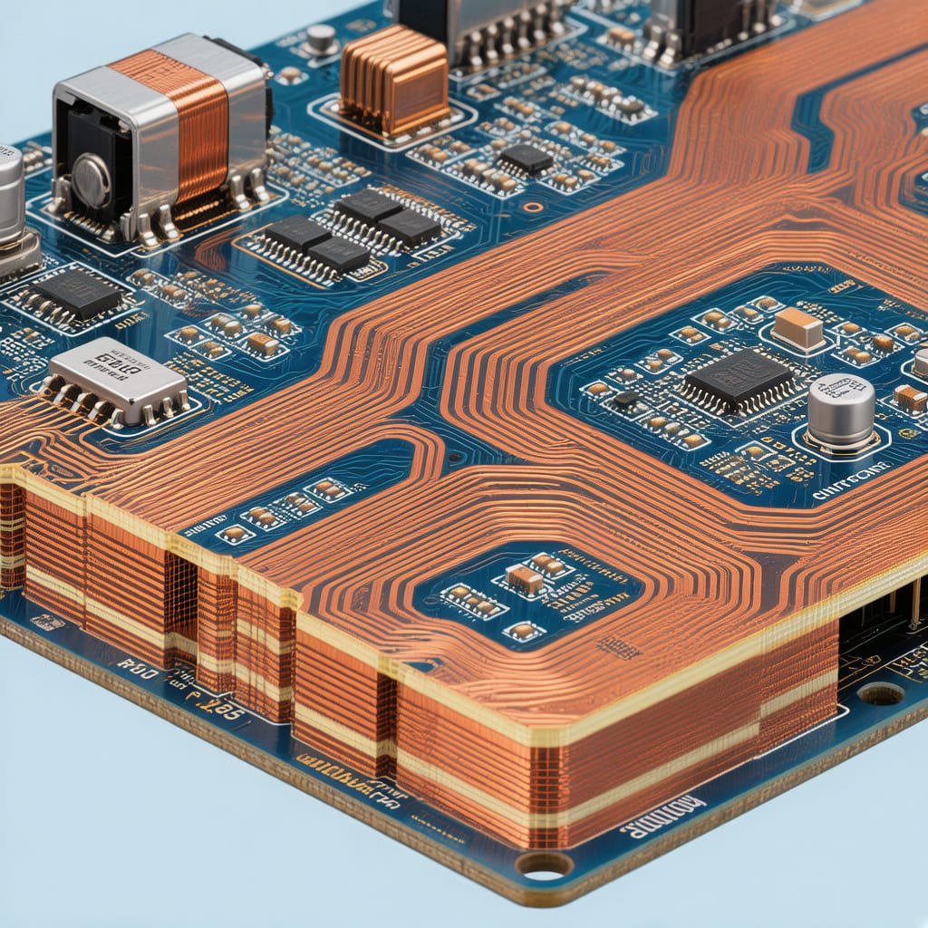
When PCB trace current exceeds 20 amperes, standard 1oz (35 μm) or 2oz (70 μm) copper becomes thermally and electrically inadequate. Heavy copper PCBs — defined as boards with 3oz (105 μm) to 10oz (350 μm) or more of copper on outer layers — bridge the gap between conventional PCBs and busbar assemblies, enabling direct SMT mounting of high-power semiconductors while handling currents that would melt standard traces.
This guide covers the practical engineering decisions involved in specifying, designing, and assembling heavy copper PCBs for power electronics applications, with particular attention to the SMT assembly challenges unique to thick copper substrates.
Copper Weight and Current Capacity: Beyond IPC-2152
The IPC-2152 standard provides conservative current-carrying capacity charts for conductors from 0.5oz to 3oz copper. For heavy copper (4oz and above), these charts become increasingly conservative because they assume uniform trace heating without accounting for the enhanced lateral heat spreading that thick copper provides.
Practical current capacity for a 10°C temperature rise above ambient (external layer, 25°C ambient):
| Copper Weight | Thickness (μm) | 10 mm Wide Trace | 25 mm Wide Trace |
|---|---|---|---|
| 1 oz (standard) | 35 | ~8 A | ~16 A |
| 3 oz | 105 | ~18 A | ~35 A |
| 4 oz | 140 | ~22 A | ~42 A |
| 6 oz | 210 | ~30 A | ~55 A |
| 10 oz | 350 | ~45 A | ~80 A |
Note: Values are approximate for single-sided, free convection cooling. Derate by 30–40% for i
er layers. Always verify with thermal simulation for safety-critical designs.
For very high currents (>100 A per trace), consider that heavy copper traces behave more like busbars than PCB traces. The trace cross-sectional area for 10oz copper at 50 mm width is 17.5 mm² — comparable to a AWG 4 wire — and resistive heating (I²R) becomes the dominant thermal design constraint.
Design Rules for Heavy Copper PCB Layout
Minimum Trace Width and Spacing
The etching process for heavy copper is inherently less precise than for standard copper. As copper thickness increases, the etch factor (ratio of lateral etch to vertical etch) produces trapezoidal trace cross-sections rather than rectangular ones. This creates three critical design rules:
- Minimum trace/space for 3oz: 0.20 mm / 0.20 mm (standard process), 0.15 mm / 0.15 mm (advanced)
- Minimum trace/space for 6oz: 0.35 mm / 0.35 mm (standard), 0.25 mm / 0.25 mm (advanced)
- Minimum trace/space for 10oz: 0.50 mm / 0.50 mm (standard), 0.35 mm / 0.35 mm (advanced)
The trapezoidal cross-section means a trace designed at 0.5 mm width on the artwork will be approximately 0.35 mm at the base after etching. Always confirm minimum etched width with your fabricator’s DFM review.
Via Design for Heavy Copper
Standard plated through-holes with 25 μm barrel plating are inadequate for heavy copper layers. Two approaches address this:
1. Copper-filled vias: Electroplated copper fill provides solid, low-resistance vertical interco
ects. Minimum drill diameter is typically 0.3 mm for 3oz and 0.5 mm for 6oz+ copper. Copper-filled vias handle 3–5× the current of standard plated vias of the same diameter.
2. Multiple parallel vias: Instead of one large via, use an array of smaller vias. Four 0.3 mm vias in parallel provide lower total resistance and better heat distribution than a single 1.0 mm via, while being easier to manufacture consistently.
Solder Mask on Heavy Copper
The height difference between the copper surface and the laminate surface creates solder mask application challenges. For 6oz+ copper, the 210 μm step height can cause solder mask thi
ing at trace edges, leading to exposed copper and potential short circuits. Solutions include:
- Two-stage solder mask application: Apply a first coat to fill the low areas, cure, then apply a second full-coverage coat
- Increased solder mask clearance: Expand solder mask openings by 0.05–0.1 mm beyond standard design rules to account for registration tolerance over the 3D surface
- Polyimide coverlay: For extreme heavy copper (8oz+), consider flexible-circuit-style polyimide coverlay instead of liquid photoimageable solder mask
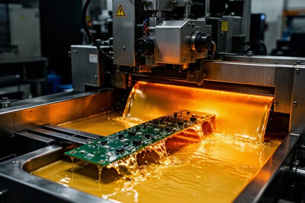
SMT Assembly Considerations
Heavy copper PCBs present unique challenges for SMT assembly that standard process parameters do not address:
Thermal mass and reflow profiling: A 6oz copper board has approximately 6× the thermal mass of an equivalent 1oz board in copper layers. This means reflow ovens must deliver significantly more energy to achieve proper peak temperatures. Profile the board with thermocouples at multiple locations — the thermal gradient across a heavy copper board during reflow can exceed 15°C, compared to 5–8°C for standard PCBs.
Recommended reflow adjustments:
- Increase soak zone duration by 30–60 seconds to allow the heavy copper mass to reach thermal equilibrium
- Reduce belt speed by 15–25% from standard settings
- Consider bottom-side convection enhancement if the oven supports it
- Peak temperature target: 235–245°C measured at the coldest pad (usually a large copper pour), not the hottest component
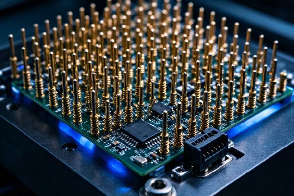
Component placement: Heavy copper boards are stiffer and flatter than standard PCBs, which generally improves pick-and-place accuracy. However, the high thermal conductivity can cause solder paste to dry out faster during extended placement cycles. Minimize the time between paste printing and reflow to under 4 hours in production environments.
When to Choose Heavy Copper vs Alternative Approaches
Heavy copper PCBs are the right choice when:
- Continuous current exceeds 20 A per trace and PCB-integrated conductors reduce assembly steps versus external busbars
- Space constraints prevent using wider traces — thick copper achieves current capacity in less board area
- Thermal management benefits from spreading heat through the copper itself (e.g., power LED boards, motor controllers)
- Mechanical strength is required — 6oz+ copper layers add significant rigidity and serve as integral heatsinks
Consider alternatives when:
- Fine-pitch SMT (<0.5 mm) is required on the same layer as heavy copper — the etch resolution conflict is fundamental
- Board flexing is expected — heavy copper creates high-stress interfaces with standard-thickness i
er layers
- Cost is the dominant constraint — heavy copper PCBs cost 2–5× more than standard equivalents due to longer etching time and lower panel utilization
For power electronics designers in the Southeast Asian manufacturing ecosystem, heavy copper PCBs represent a mature, well-supported technology with established supply chains. The key to success lies not in exotic design rules but in disciplined DFM communication with the fabricator and willingness to adjust SMT process parameters to accommodate the thermal realities of thick copper substrates.