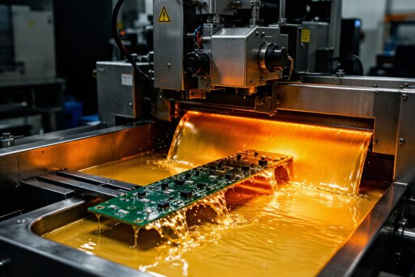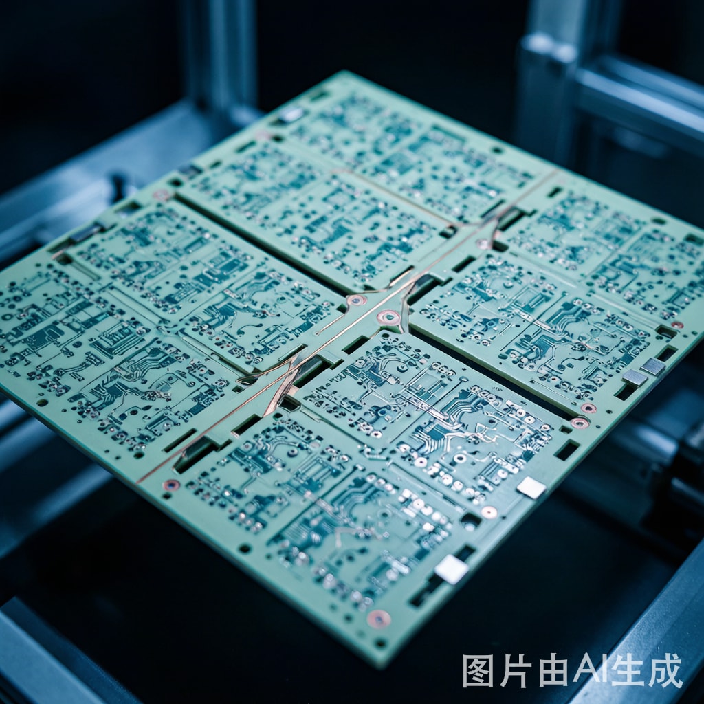
For high-volume SMT production, individual PCBs almost never travel down the assembly line as single boards. Instead, they are panelized — multiple identical units arrayed on a larger manufacturing panel — to maximize pick-and-place throughput, reduce handling time, and enable automated optical inspection at the array level. The two dominant panelization methods are V-cut (V-scoring) for rectangular boards and tab-routing (breakaway tabs) for complex shapes. When V-cut is the right choice, the geometry of the V-groove itself becomes a critical factor in downstream yield.
V-Cut Geometry Fundamentals
A V-cut is created by a saw blade with a conical or wedge-shaped tip that cuts a controlled-depth groove on both top and bottom surfaces of the panel along the intended separation line. When all components on both sides of the groove are placed and reflowed, the boards are separated by flexing the panel along the V-scored line until the remaining web of material fractures.
Three geometric parameters define a V-cut:
- Top-side cut depth: Distance from top surface to bottom of the V-groove. Typical: 0.3–0.5 mm for a 1.6 mm thick board (18–30% of thickness).
- Bottom-side cut depth: Same measurement from bottom surface. Should mirror top side to within ±0.05 mm.
- Remaining web thickness: The unbroken material between top and bottom cuts. This is the critical parameter — too thick and the board ca
ot be cleanly separated; too thin and the panel becomes fragile during assembly.
Standard web thickness: 0.3–0.4 mm for 1.6 mm boards, 0.4–0.5 mm for 2.0 mm boards. Boards with component overhang across the V-scored line should target web thickness 0.4–0.5 mm to prevent cracking into adjacent components during separation.
V-Cut Angle and Tooling
The V-cut angle (apex angle of the groove) is determined by the saw blade profile. Common blade angles are:
- 30° included angle: Standard for general-purpose V-cut. Produces a sharp groove that cleanly separates with moderate bending force.
- 45° included angle: Used for thicker boards (≥2.0 mm) or when higher breakaway strength is needed during assembly. Requires more force to separate but is more resistant to accidental cracking.
- 60° included angle: Specialized use for very thick boards (≥3.2 mm) or when the V-cut must also serve as a fiducial alignment feature.
For SMT production environments, the 30° blade is overwhelmingly the most common. Its separation force falls in the 5–15 N range — well within manual handling capability while remaining stable through the assembly process.
Edge Distance and Component Clearance
The V-cut groove removes material to within 0.3–0.5 mm of the board surface. Any copper feature, component pad, or SMT part placed within this zone is at risk of damage during separation. Critical clearance rules:
| Feature | Minimum Distance from V-Cut Center Line | Rationale |
|---|---|---|
| Copper trace (any layer) | 0.5 mm | Prevent crack propagation into trace |
| SMT component pad | 1.0 mm | Avoid pad lifting during flex |
| Component body | 1.5 mm (0.5 mm preferred) | Mechanical clearance during breakaway |
| Test point / fiducial | 1.0 mm | Preserve probe access after depanelization |
| Solder mask opening | 0.4 mm from groove edge | Prevent mask peel-back |
For BGAs or fine-pitch components, designers often route V-cuts between component placement areas rather than across them. The classic panel layout places V-cuts along a 2×2 or 3×3 grid of identical boards, with the V-cuts ru
ing through empty board real estate rather than through component zones.
Edge Plating: When and Why
Edge plating (also called side plating or castellated holes) refers to plated copper that wraps around the board edge, providing electrical co
ection between top-layer, bottom-layer, and the cut edge. The primary applications are:
- EMI shielding continuity: When a board edge forms part of an enclosure seam, edge plating ensures the top-side ground plane, bottom-side ground plane, and any side-mounted shield contact are all at the same potential.
- Board-to-board edge co
ectors
: Castellated holes along the board edge allow a daughter board to be soldered directly onto a mother board, creating a solder-down card-edge coection without a separate co
ector. Common in IoT modules, LED strips, and embedded controller boards.
- Heat dissipation: Edge plating on a power-converter board can extend the copper thermal path around the board edge to a heatsink mounted on the side.
Edge plating requires that the V-cut or routing cut leave a clean, square edge on which the plating can adhere. V-cuts, due to their angled geometry, are not ideal for edge plating — the beveled surface provides only limited plating contact area. For edge-plated designs, tab-routing with plated stub edges is the preferred panelization method.
V-Cut vs Tab-Routing: Selection Criteria
Choose V-cut when:
- Board shape is rectangular with all four edges straight
- Component spacing from edges is ≥1.5 mm (no tight clearances)
- Edge plating is not required
- Throughput is critical — V-cut panels separate in 1–2 seconds vs 10–30 seconds for tab-routing with hand depanelization
- Panel size is large (e.g., 200×250 mm arrays of 4–9 boards)
Choose tab-routing when:
- Board has irregular outline (cutouts, rounded corners, non-rectangular shapes)
- Edge plating is required on any edge
- Component clearance from edges is <1.0 mm (V-cut would risk damage)
- Mechanical stress during separation must be minimized (rigid-flex, ceramic substrates, large BGAs)
- Low-volume production where the additional routing cost is amortized over few panels
Depanelization Methods and Stress Control
The moment of separation is when V-cut panels are most vulnerable to inducing latent defects. The three principal depanelization methods, in increasing order of stress:
- Manual hand-break: Operator holds the panel on both sides of the V-cut and applies bending force. Skill-dependent, but properly executed produces clean breaks. Risk: inconsistent force application may over-stress the area near the V-cut on the board, particularly affecting large ceramic capacitors or BGAs within 5 mm of the V-cut line.
- Pneumatic depanelizer: Press applies controlled force at the V-cut line, separating the panel with consistent bending radius. Reduces operator variability. Typical cycle time 2–4 seconds per V-cut line.
- Inline router / laser depanelizer: CNC router or CO₂/UV laser cuts through the V-cut web rather than bending. Eliminates bending stress entirely but adds 5–15 seconds per separation and requires capital investment of $40,000–$200,000 for the equipment.
For products with large BGAs near the board edge (>10 mm BGAs within 5 mm of V-cut), the inline router or laser method is strongly recommended. Manual or pneumatic bending can introduce micro-cracks in BGA solder joints that survive reflow but fail prematurely in thermal cycling — a defect that is invisible at ICT but shows up as field returns within months of deployment.
Quality Verification
V-cut panel quality should be verified at three stages:
- Incoming panel inspection: Measure V-cut depth at 5 points along each scored line using a depth gauge or cross-section microscopy. Acceptance criterion: depth within ±0.05 mm of nominal, with no deviation exceeding ±0.10 mm. Reject any panel with V-cut intrusion into the top or bottom copper layer.
- Pre-assembly coplanarity: After SMT placement and reflow, measure board flatness on the panel. Excess warpage introduced by uneven V-cut stress concentration can exceed pick-and-place Z-axis tolerance.
- Post-depanelization inspection: Examine the separated board edge under 10× magnification. Acceptable edge shows clean fracture with no copper pull-back, no delamination extending more than 0.2 mm into the board, and no component damage within 2 mm of the V-cut line.
For high-volume SMT operations, V-cut panelization remains the most cost-effective depanelization method for rectangular boards. The discipline is to treat the V-cut as a designed feature with clear DFM rules — not as a post-layout afterthought added by the fabricator. Engaging fabrication partners early in the layout process, with explicit specification of V-cut depth, blade angle, edge distances, and depanelization method, is the single most effective way to avoid the late-stage surprises that turn efficient panelization into costly rework.