Introduction
High Density Interco
ect (HDI) microvias have become the foundation of modern mobile, wearable, and IoT electronics. As smartphones pack more functionality into smaller form factors, and IoT devices demand miniaturized sensor nodes with wireless co
ectivity, HDI technology with stacked microvias is no longer optional — it is essential. However, the reliability of these tiny interco
ects (typically 50-150 µm in diameter) depends on careful control of design rules, manufacturing processes, and acceptance criteria per IPC-6012.
What Makes a Microvia Different
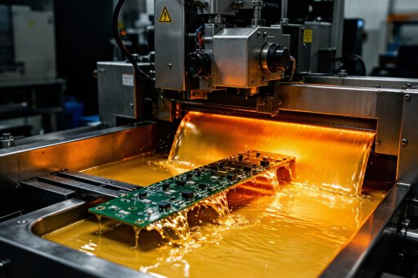
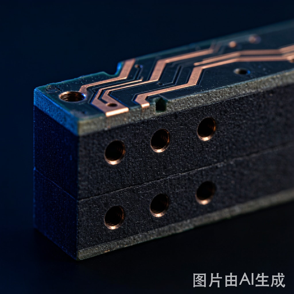
A microvia is defined by IPC as a blind or buried via with a diameter of 150 µm or less, typically formed by laser drilling rather than mechanical drilling. The most common fabrication approach uses CO₂ or UV laser ablation to create a conical or cylindrical hole in the dielectric material, exposing the copper pad of the layer below. The hole is then metallized with electroless copper, followed by electrolytic plating to build up the via barrel.
Unlike conventional through-holes, microvias co
ect only two adjacent layers. This limits their aspect ratio to approximately 0.75:1 for reliable copper plating — a 100 µm diameter microvia can be reliably plated only through approximately 75 µm of dielectric thickness. This constraint shapes the entire HDI stack-up design.
Stacked vs Staggered Microvia Configurations
When routing density requires multiple layer transitions in close proximity, designers face a choice between two microvia configurations:
Stacked Microvias
Stacked microvias place one microvia directly on top of another, sharing the same copper land pad. This configuration maximizes routing density and is the standard for any-layer HDI designs used in smartphones and advanced wearables. The manufacturing challenge is ensuring robust copper plating through the stacked structure — any defect in the lower via propagates to the upper via, creating a single point of failure.
Staggered Microvias
Staggered microvias offset each via by at least one pad diameter, so the upper via lands on a separate copper plane rather than directly on the lower via. This configuration is inherently more reliable because each via is independently anchored, but it consumes more board real estate. Staggered microvias are typical in IoT devices, automotive electronics, and industrial control modules where reliability outweighs routing density.
Reliability Failure Mechanisms
The primary reliability concerns for HDI microvias are:
- Barrel cracking — Caused by thermal cycling stress concentrated in the copper barrel. CTE mismatch between copper (17 ppm/°C) and dielectric (60-70 ppm/°C for typical FR-4) creates cyclic strain at the via interface. Stacked microvias are particularly susceptible because the stress concentrations compound across multiple interfaces.
- Land pad separation — Where the microvia lands on the target copper pad, the interfacial bond can delaminate if the capture pad is too small or if electroless copper adhesion is insufficient. This is the dominant failure mode for staggered microvia designs.
- Dimple formation — During the laser drilling process, the dielectric material around the via entrance can recess slightly, creating a small dimple that traps air and impairs subsequent plating. Proper desmear and electroless copper deposition are critical to eliminate this defect.
- I
er-layer misregistration
— The capture pad must be larger than the laser spot size plus manufacturing tolerance. Under-sized capture pads expose the dielectric at the via base, creating an unreliable interface.
Copper Filling for Stacked Structures
Why Copper Filling Matters
For stacked microvia designs in Class 3 applications (medical, aerospace, mission-critical), the microvias must be filled with copper — not just plated. Copper filling eliminates the air gap that would otherwise be trapped between stacked vias, providing a continuous solid copper column that can carry current, dissipate heat, and resist thermal cycling stress.
Filling Process Steps
- Drill and desmear the microvia
- Deposit electroless copper as a plating base (0.5-1.0 µm)
- Apply electrolytic copper using a specialized microvia-filling chemistry with organic additives (suppressors and accelerators) that promote bottom-up filling
- Planarize the surface through controlled micro-etching or fly-cutting
- Apply surface finish (ENIG, ENEPIG, OSP)
Well-controlled copper filling produces a void-free via with less than 5% dimple depth. Any void or significant dimple disqualifies the via for stacked HDI applications.
IPC-6012 Acceptance Criteria
IPC-6012 defines three performance classes for HDI microvia structures, with progressively tighter acceptance limits:
- Class 1 (General Electronic Products) — Permits dimple depths up to 25% of dielectric thickness and barrel thickness of 5 µm minimum
- Class 2 (Dedicated Service Electronic Products) — Requires dimple depth below 20% and barrel thickness of 8 µm minimum, with no voids in the dielectric interface
- Class 3 (High Reliability Electronic Products) — Demands dimple depth below 10%, barrel thickness of 12 µm minimum, void-free copper filling for stacked structures, and 100% automated optical inspection of all microvias
For mobile and IoT products, most manufacturers target Class 2 acceptance as a baseline, with Class 3 reserved for medical devices, automotive safety systems, and aerospace applications.
Design Guidelines Summary
- Microvia diameter: 75-125 µm for 1+N+1 HDI; 50-100 µm for 2+N+2 any-layer HDI
- Dielectric thickness: 40-80 µm between microvia layers to maintain reliable plating aspect ratio
- Capture pad diameter: at least 1.5× the microvia diameter for Class 2, 1.75× for Class 3
- Pad-to-pad spacing for staggered microvias: minimum one microvia diameter between capture pads
- Aspect ratio: not greater than 0.75:1 (depth to diameter) for reliable electroless plating
Conclusion
HDI microvia reliability is not a single design choice but a system of interrelated decisions spa
ing stack-up architecture, laser process control, copper filling chemistry, and acceptance criteria. For mobile and IoT applications, the balance between routing density and long-term reliability typically favors stacked microvia structures with copper filling per IPC-6012 Class 2 or Class 3 standards. Investing in tight design rules and robust process controls during NPI prevents costly field failures and product recalls across the product lifecycle.