Introduction
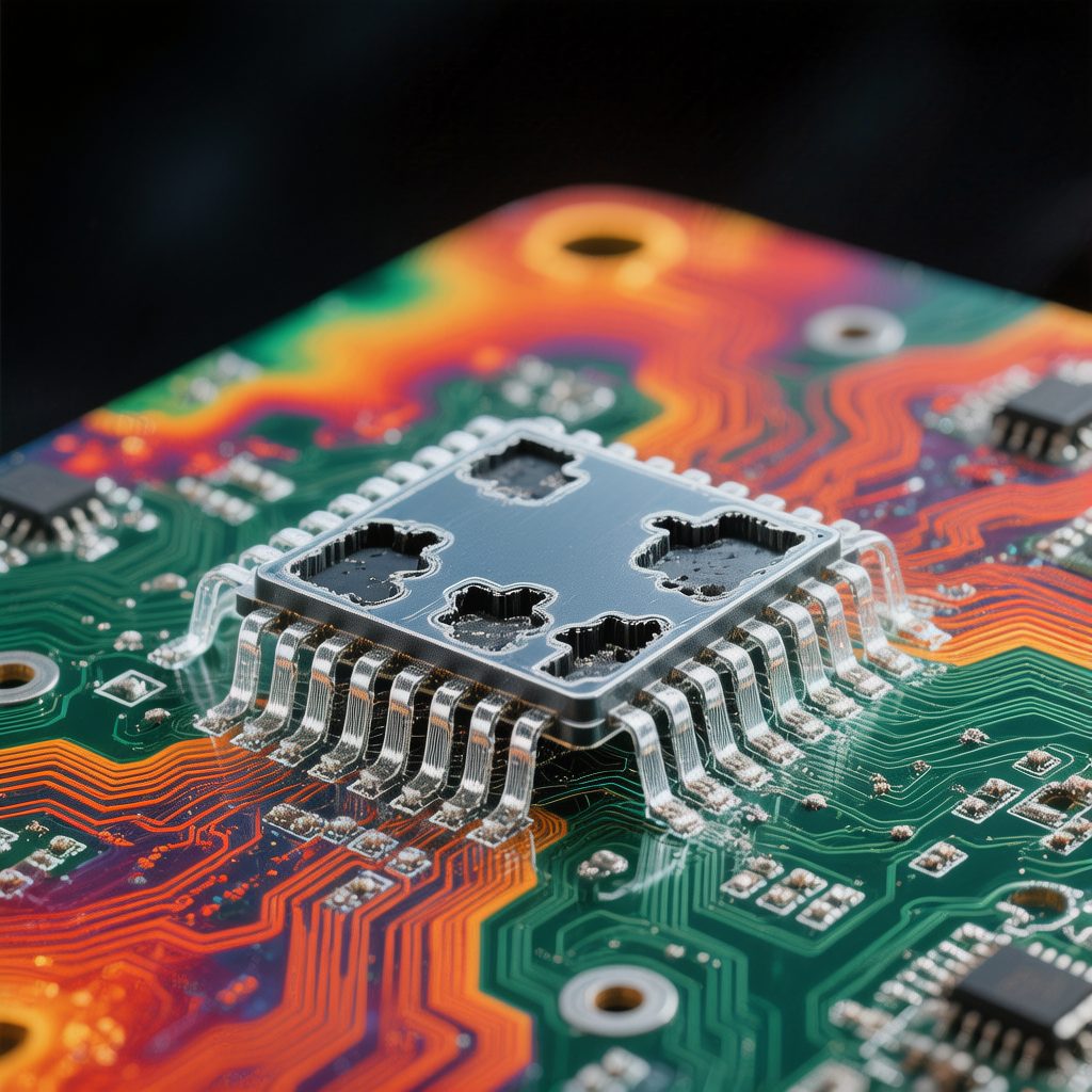
Solder void formation beneath bottom-terminated components (BTCs) — including QFN, DFN, LGA, and exposed-pad packages — is one of the most persistent challenges in SMT assembly. Voids in the thermal pad solder joint increase thermal resistance, reduce mechanical reliability, and can cause device overheating or premature failure. IPC-7093 recommends void rates below 25% for Class 1 and 2, and below 10% for Class 3 assemblies, yet achieving these targets consistently requires systematic process optimization.
Root Causes of Void Formation
Understanding void formation mechanisms is essential before implementing solutions. The primary causes include:
- Outgassing — Flux volatiles trapped beneath the component ca
ot escape through the narrow standoff gap (typically 50-100 µm for QFN packages). As the solder melts, these gases expand and form spherical voids.
- Poor wetting dynamics — If the solder paste does not wet the pad and component termination uniformly, entrapped flux pockets create irregular void patterns.
- Oxide contamination — Oxidized pad surfaces or component terminations inhibit wetting, creating void-prone regions where solder fails to coalesce properly.
- Stencil design limitations — Inadequate aperture coverage or geometry prevents flux from escaping the solder joint during reflow.
Stencil Aperture Design Optimization
The stencil aperture pattern for the thermal pad is the single most influential factor in void reduction. Rather than using a single large aperture, segmenting the thermal pad into multiple smaller openings — typically in a window-pane or grid pattern — creates cha
els for flux outgassing.
A well-designed segmented stencil achieves 50-70% solder paste coverage of the thermal pad area. The apertures should be sized so that individual solder deposits coalesce during reflow while maintaining escape paths for volatiles. Common configurations include:
- 3×3 or 4×4 grid of square apertures with 0.3-0.5 mm spacing between them
- Circular aperture arrays with 0.4-0.6 mm diameter and staggered arrangement
- S-shaped or serpentine apertures that maximize perimeter-to-area ratio for outgassing
Stencil thickness should be 100-127 µm (4-5 mil) for fine-pitch QFN packages. For larger thermal pads, step-up stencils with 150 µm thickness over the thermal pad area can increase solder volume without compromising fine-pitch printing quality.
Solder Paste Selection
Solder paste chemistry directly influences voiding behavior. Key considerations include:
Flux type: No-clean pastes formulated for low-voiding applications contain flux systems designed to volatilize completely before solder melting. Look for pastes specifically marketed as “low-voiding” or “QFN-optimized” — these typically use high-boiling-point solvents that remain liquid until just before solder liquidus, then escape rapidly.
Powder size: Type 4 (20-38 µm) or Type 5 (15-25 µm) powder provides better print definition for fine-pitch QFN peripherals while maintaining adequate metal content for thermal pad coverage. The finer powder also improves coalescence dynamics, reducing the likelihood of trapped flux pockets.
Reflow Profile Optimization
The reflow profile significantly influences void formation and escape. A longer soak zone (60-90 seconds above 150°C) allows flux activators to fully clean oxide surfaces and begin volatilization before solder melting. The time above liquidus (TAL) should be carefully controlled:
For SAC305 solder paste, a peak temperature of 240-245°C with 60-90 seconds TAL provides sufficient time for voids to migrate to the periphery and escape. Some manufacturers report improved results with a “soak-and-spike” profile: extended soak at 180-200°C followed by rapid ramp to peak, which creates thermal gradients that help drive voids outward.
Vacuum Reflow Technology
For Class 3 assemblies where void rates below 5% are required, vacuum reflow ovens provide the most reliable solution. By reducing chamber pressure to 10-50 mbar during the liquidus phase, the pressure differential between the void interior and the vacuum environment forces trapped gas out of the solder joint. Vacuum reflow consistently achieves void rates below 2% for QFN packages, though at significantly higher equipment cost compared to atmospheric reflow.
Conclusion
Reducing solder voids in bottom-terminated components requires a multi-faceted approach combining optimized stencil design, low-voiding solder paste, and precisely controlled reflow profiles. Segmented stencil apertures remain the most cost-effective starting point, often reducing void rates from 30-40% to below 15% without any other process changes. For applications demanding void rates below 5%, vacuum reflow technology provides the ultimate solution. Regular X-ray inspection and statistical process control ensure these improvements are sustained across production volumes.