Introduction
As SMT power electronics continue to push toward higher current densities, PCB designers face a critical decision: route high current through heavy copper PCB traces or integrate discrete copper busbars. Both approaches have valid applications, but choosing incorrectly can lead to thermal runaway, voltage drop issues, and costly redesigns. This article provides a data-driven comparison to help you make the right choice for your next power electronics design.
Understanding Current Density Limits
The fundamental constraint in any high-current design is current density, typically expressed in A/mm². Standard 1 oz (35 µm) copper traces can handle approximately 1-3 A/mm² with a 10°C temperature rise, depending on trace width and ambient conditions. Heavy copper PCBs using 4-10 oz copper can push this to 10-20 A per trace, but the relationship is not linear.
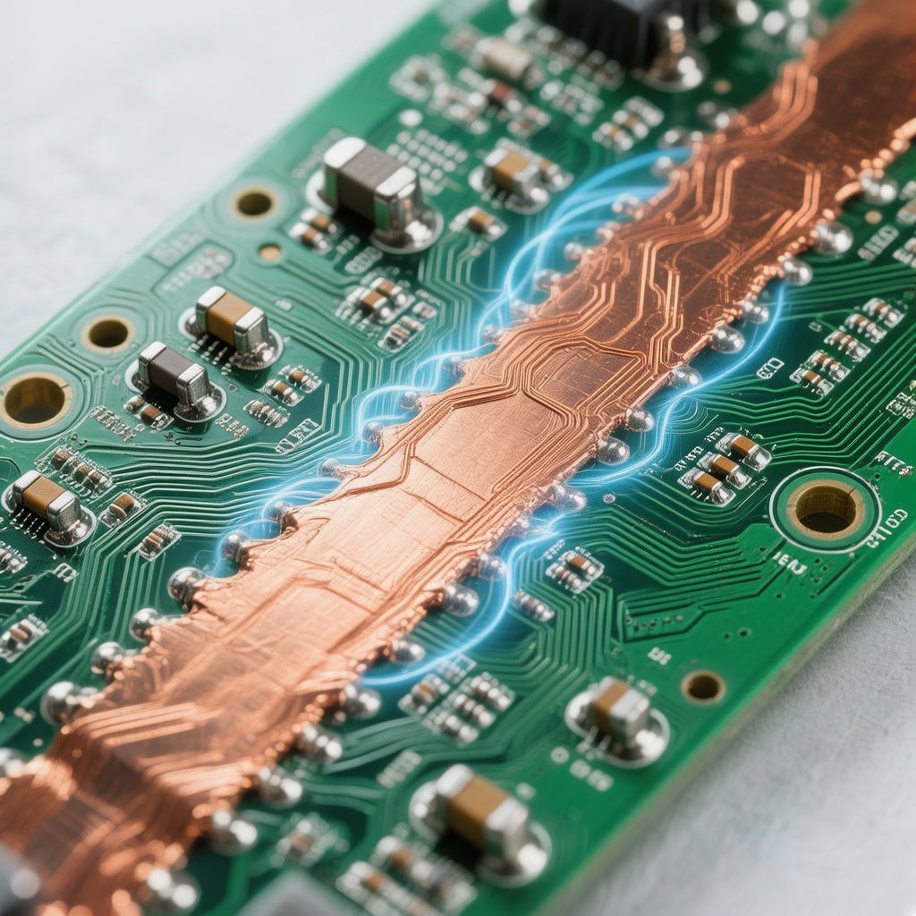
Copper busbars, by contrast, are typically fabricated from high-conductivity electrolytic tough pitch (ETP) copper with cross-sections measured in square millimeters rather than microns. A modest 5 mm × 2 mm busbar provides a 10 mm² cross-section — equivalent to approximately 285 ounces of PCB copper. This orders-of-magnitude difference in cross-sectional area is the primary reason busbars dominate in applications exceeding 100 A.
Thermal Management Considerations
I²R losses generate heat proportional to the square of current multiplied by resistance. For a 50 A circuit with 2 mΩ trace resistance, that is 5 W of heat concentrated along the trace path. In a dense SMT assembly, this localized heating can elevate component junction temperatures beyond rated limits.
Copper busbars serve dual purpose as both conductors and heat spreaders. Their substantial thermal mass and surface area dissipate heat more effectively than PCB traces, which are thermally coupled to the FR-4 substrate — a relatively poor thermal conductor at approximately 0.3 W/m·K. For designs where both electrical and thermal paths are critical, busbars often provide a more elegant solution than adding separate heatsinks.
Thermal Comparison Table
| Parameter | 4 oz PCB Trace (10 mm wide) | 5×2 mm Copper Busbar |
|---|---|---|
| Cross-sectional Area | 1.4 mm² | 10 mm² |
| Resistance @ 25°C (per 100 mm) | ~1.2 mΩ | ~0.17 mΩ |
| Max Continuous Current (40°C rise) | ~35 A | ~150 A |
| Heat Dissipation Path | Through FR-4 substrate | Direct convection/radiation |
Manufacturing and Assembly Tradeoffs
Heavy copper PCBs require specialized etching processes. Copper thickness above 4 oz demands longer etch times and can cause undercut — where the etchant attacks copper beneath the photoresist, reducing trace width accuracy. This limits minimum trace/space capabilities and increases PCB cost significantly.
Busbar integration introduces assembly complexity. Busbars must be mechanically fixtured during SMT reflow or added as a secondary assembly step using screws, press-fit pins, or selective wave soldering. However, modern SMT-compatible busbars with solderable surface finishes (tin-plated, nickel-plated, or ENIG) can be placed and reflowed alongside other components, streamlining the assembly process.
When to Choose Each Approach
Choose Heavy Copper PCB Traces When:
- Current is below 50 A per net
- Board space is constrained and busbar mounting points are impractical
- The design is high-volume with automated assembly as the priority
- Multiple high-current nets require complex routing patterns
Choose Copper Busbars When:
- Current exceeds 50 A continuously
- Voltage drop must be minimized (below 50 mV at full load)
- Thermal management is a primary concern
- The busbar can also serve as a structural or mounting element
- Design calls for a combination of high current and low inductance
Hybrid Approaches
Many modern power designs employ a hybrid strategy: heavy copper i
er layers for moderate current distribution combined with external busbars for the highest current paths. This approach optimizes both board real estate and thermal performance. Embedded copper coin technology can also bridge the gap, placing thick copper elements within the PCB stack-up for localized high-current zones.
Conclusion
The choice between copper busbars and heavy copper PCB traces is not binary — it is a spectrum of solutions tailored to current requirements, thermal budgets, and manufacturing constraints. Understanding the current density limits and thermal behavior of each approach allows you to optimize your SMT power electronics design for reliability and cost-effectiveness. For applications pushing beyond 50 A, copper busbars consistently deliver superior electrical and thermal performance with manageable assembly tradeoffs.