Why PCB Warpage During Reflow Is a Yield Killer
PCB warpage under reflow temperatures is one of the most insidious yield detractors in SMT assembly—one that often goes undiagnosed until the first-article inspection reveals a trail of BGA opens, QFN head-in-pillow defects, and passive component tombstoning. The root cause is the differential thermal expansion between copper layers, glass-reinforced laminate, and the resin matrix, all compounded by asymmetric layer stack-ups and uneven copper distribution.
When a PCB exceeds the IPC-6012 flatness threshold of 0.75% for surface-mount boards (measured as bow percentage over the diagonal span), the probability of open solder joints at BGA corners increases exponentially. This article covers the engineering fundamentals of PCB warpage in SMT reflow, from copper balance design to material selection and in-process measurement.
Understanding the Mechanics of PCB Warpage at Reflow Temperature
FR-4 laminate is a composite of woven glass fabric and epoxy resin. Below its glass transition temperature (Tg), the laminate exhibits a coefficient of thermal expansion (CTE) of approximately 14–17 ppm/°C in the X-Y plane and 50–70 ppm/°C in the Z-axis. Above Tg—right in the SAC305 peak reflow zone of 235–250°C—the Z-axis CTE jumps to 250–350 ppm/°C.
Now consider what happens on a typical 6-layer PCB: if the i
er layers carry heavily unbalanced copper distribution—say, a 70% copper fill on layer 2 versus 20% on layer 5—the differential in-plane expansion creates a bending moment that manifests as warpage at reflow temperature. The board curves concave or convex, lifting critical BGA corner balls away from the solder paste deposit.
Copper Balance: The First Line of Defense
Copper distribution symmetry across the board cross-section is the most effective design-level countermeasure against reflow-induced warpage. Key practices include:
- Layer pair balancing: Each signal/plane layer pair (e.g., L2–L5, L3–L4) should have copper coverage within 15% of each other. Use copper thieving patterns on sparse layers to add dummy fill.
- Symmetrical stack-up: The dielectric thickness and copper weight should be mirror-symmetric about the center plane. A 6-layer board with the stack-up Prepreg-Core-Prepreg-Core-Prepreg must have identical prepreg types on both sides.
- Thermal relief pad design: Thermal relief spokes on copper planes reduce the plane-to-pad CTE mismatch by allowing controlled expansion relief around through-hole pads and vias.
IPC-TM-650 Warpage Measurement Methods
IPC-TM-650 2.4.22 defines the standard method for measuring PCB bow and twist. The measurement involves placing a bare board on a flat granite surface and using a height gauge or profilometer to record the maximum vertical deviation from the reference plane. Measurements are taken at room temperature and at simulated reflow temperature using a shadow moiré system.
Shadow Moiré Thermomechanical Analysis
Shadow moiré is the gold standard for dynamic warpage measurement. A diffraction grating is placed above the PCB inside a thermal chamber, and a light source projects fringe patterns onto the board surface. As the temperature ramps through the reflow profile, the fringe distortion quantifies out-of-plane displacement with micron-level resolution. This technique captures the critical “warpage at liquidus” condition—when solder is molten and has zero mechanical restraint against PCB movement.
A well-designed board typically shows less than 0.5% bow at 230°C, while poorly balanced designs can exceed 1.5%, at which point BGA open defect rates rise above 5,000 PPM.
Material Selection for Warpage Control
Beyond copper balance, the laminate material itself plays a decisive role:
- High-Tg FR-4 (Tg ≥ 170°C): Delays the CTE jump to a higher temperature, reducing the time the board spends in the high-CTE regime during reflow. Suitable for most consumer and industrial electronics.
- Polyimide laminates (Tg ≥ 250°C): Minimal CTE change through the entire lead-free reflow window. Used in aerospace, military, and high-reliability automotive applications.
- Low-CTE glass fabrics: S-glass and quartz-reinforced laminates offer X-Y CTE as low as 6–8 ppm/°C, dramatically reducing in-plane expansion mismatch with copper (17 ppm/°C).
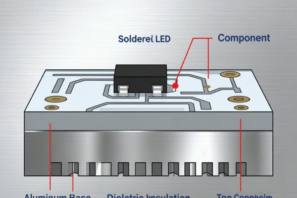
- Metal-core PCBs (aluminum/copper base): The metal substrate acts as a mechanical stiffener, virtually eliminating warpage. Common in LED lighting and high-power applications.
Process-Level Mitigation Strategies
Even with a well-designed board, process controls can mitigate residual warpage:
- Reflow carrier/pallet support: Custom-machined aluminum or titanium carriers hold the PCB flat during reflow. Essential for boards thi
er than 1.0 mm.
- Reduced peak temperature: Operating at the lower end of the SAC305 liquidus range (235°C instead of 250°C) reduces thermal stress while maintaining reliable solder joint formation.
- Oven zone profiling: A gradual ramp rate of 1.5–2.0°C/s through the preheat and soak zones minimizes thermal shock that can trigger asymmetric warpage.
- Panel design with breakaway tabs: For panelized boards, strategically placed breakaway tabs and routed slots relieve stress accumulation during reflow.
Case Example: BGA Warpage Root Cause Analysis
A contract manufacturer experienced a 3.2% open-joint rate on a 784-ball BGA with 0.8 mm pitch. Shadow moiré analysis revealed 1.8% bow at 240°C—well above the IPC limit. Investigation found that layer 3 (ground plane) had 85% copper coverage while layer 8 (power plane) had only 22%. Adding copper thieving to layer 8 brought both layers to approximately 45% coverage, reducing measured bow to 0.42% and eliminating BGA defects.
Conclusion
PCB warpage during SMT reflow is a design-manufacturing interface problem. The most effective solutions combine copper balance symmetry in the stack-up, appropriate laminate material selection, and process-level controls like reflow carriers. Investing in shadow moiré analysis during NPI (new product introduction) pays for itself by preventing reflow-related defects before they reach volume production.