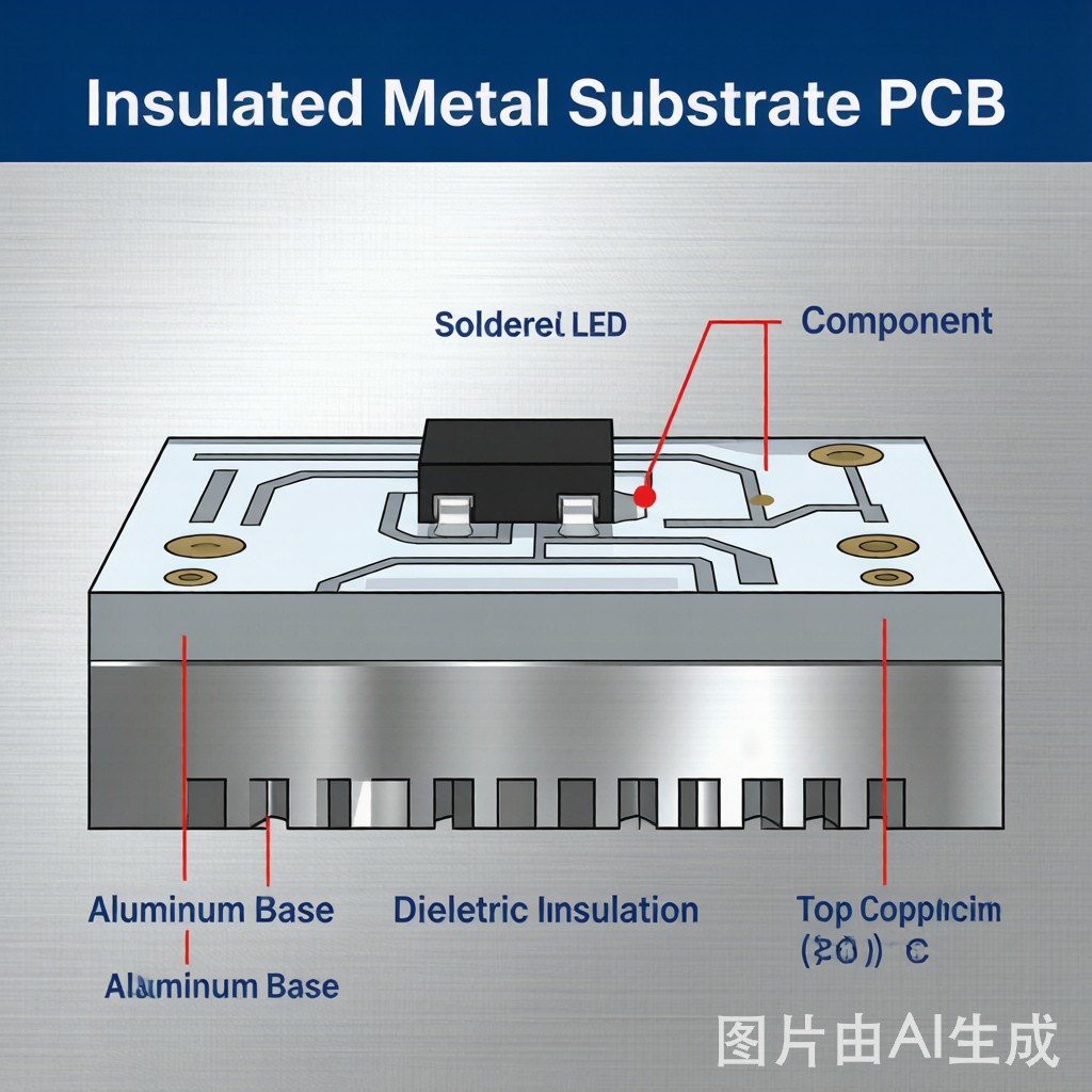
High-power LED assemblies present a thermal management challenge that conventional FR-4 PCBs ca
ot solve. A single 5 W high-brightness LED produces 1.5 W or more of waste heat, and keeping the LED junction temperature below its rated maximum (typically 125–150°C for most LEDs, lower for high-CRI or high-power parts) requires a thermal path from the LED die to a heatsink with a total thermal resistance of < 5°C/W. The standard FR-4 PCB, with its thermally insulating fiberglass-epoxy substrate, has a thermal resistance of 1.5–3.0°C/W per square centimeter of board — which means a 1 cm² LED footprint alone, before any TIM or heatsink, would add 3°C to the junction temperature. Insulated Metal Substrate (IMS), also called metal-core PCB (MCPCB) or thermal-clad PCB, replaces the FR-4 with a metal base (typically aluminum or copper) that dramatically reduces this thermal resistance.
IMS Layer Stack-Up
A standard IMS stack-up consists of three layers:
- Metal base layer: Aluminum (most common) or copper, typically 0.8–3.2 mm thick. Aluminum is the standard choice for cost-sensitive LED applications; copper is used when higher thermal conductivity or specific thermal expansion matching is required.
- Dielectric layer: A thin, thermally conductive but electrically insulating layer, typically 35–200 μm thick. Common dielectric materials are filled epoxy, filled polyimide, or filled ceramic. The dielectric’s thermal conductivity (1.0–7.0 W/m·K) is the most important material property determining the overall thermal performance of the IMS.
- Copper circuit layer: Standard electrodeposited copper foil, 1–4 oz (35–140 μm) thick. Single-sided circuits are most common; double-sided IMS is also manufactured for more complex designs.
The total thickness of an IMS is typically 0.8–3.2 mm, with the metal base dominating the mechanical stiffness. The substrate is significantly more rigid than FR-4, which is an advantage for mechanical mounting but a constraint for applications requiring flex or complex shapes.
Thermal Resistance Comparison
For a 1 cm² thermal pad, the thermal resistance from the LED junction side of the IMS to the metal base side is:
| Substrate Type | Construction | Thermal Resistance (°C/W per cm²) |
|---|---|---|
| FR-4 (1.6 mm, 1 oz Cu) | Standard PCB | 20–35 |
| IMS (1.5 mm Al, 75 μm dielectric) | Standard thermal-clad | 0.5–1.5 |
| IMS (1.0 mm Cu, 50 μm high-k dielectric) | High-performance IMS | 0.2–0.5 |
| Ceramic substrate (AlN, 1.0 mm) | Direct-bonded copper | 0.05–0.15 |
| Ceramic substrate (Al₂O₃, 1.0 mm) | Direct-bonded copper | 0.20–0.40 |
For a 3 W LED with 1 cm² thermal footprint, FR-4 would add 60–105°C of thermal resistance, far exceeding the LED’s thermal budget. Standard IMS reduces this to 1.5–4.5°C. High-performance IMS with copper base and high-thermal-conductivity dielectric brings it to 0.6–1.5°C. Ceramic substrates (AlN, Al₂O₃ with DBC) offer the best performance but at 10–30× the cost of IMS.
Dielectric Material Selection
The dielectric layer is the thermal bottleneck of an IMS. Standard dielectric is a filled epoxy with thermal conductivity 1.0–2.0 W/m·K. High-performance dielectrics use ceramic fillers (alumina, boron nitride, aluminum nitride) in polyimide or modified epoxy binders, achieving 3.0–7.0 W/m·K.
The thermal conductivity of the dielectric directly sets the thermal resistance of the substrate:
| Dielectric Thermal Conductivity | Thickness 75 μm | Thickness 100 μm | Thickness 150 μm |
|---|---|---|---|
| 1.0 W/m·K | 0.75 °C·cm²/W | 1.00 °C·cm²/W | 1.50 °C·cm²/W |
| 2.0 W/m·K | 0.38 | 0.50 | 0.75 |
| 3.0 W/m·K | 0.25 | 0.33 | 0.50 |
| 5.0 W/m·K | 0.15 | 0.20 | 0.30 |
| 7.0 W/m·K | 0.11 | 0.14 | 0.21 |
For high-power LED designs, the dielectric thickness and material must be selected together. A thicker dielectric provides higher electrical isolation (useful for higher-voltage LED strings) but increases thermal resistance. Standard IMS offerings balance these with 75–100 μm dielectric thickness and 2.0–3.0 W/m·K thermal conductivity.
Electrical isolation is critical for safety. The dielectric must withstand the maximum DC voltage of the LED string (typically 24–48 V for commercial LED, 380 V for high-voltage industrial LED) plus regulatory safety margin. Standard IMS dielectric withstands 2–4 kV AC; high-voltage IMS can withstand 6–8 kV AC. The breakdown voltage is independent of the dielectric’s thermal conductivity — it depends on the dielectric’s thickness, uniformity, and pinhole-free manufacturing.
Aluminum vs Copper Base
The metal base layer provides both mechanical support and thermal spreading. Two materials dominate:
Aluminum base: Standard for LED lighting and most consumer applications. Thermal conductivity 130–200 W/m·K (depending on alloy — 6061 is most common, with 1050 alloy slightly higher at 200 W/m·K). Density 2.7 g/cm³, low cost, easy to machine. Coefficient of thermal expansion (CTE) 23 ppm/°C, which is significantly higher than FR-4 (14 ppm/°C) and silicon (3 ppm/°C). This CTE mismatch is a reliability concern for high-power LEDs and is the main reason copper-base IMS exists.
Copper base: Used for high-reliability and high-power applications. Thermal conductivity 380 W/m·K for C11000 (ETP) and 350 W/m·K for C19400. CTE 17 ppm/°C, much closer to FR-4 and ceramic, reducing thermal stress on solder joints and component interfaces. Density 8.9 g/cm³ — over 3× heavier than aluminum. Cost 4–6× aluminum. The dominant choice for aerospace, automotive headlamp, and high-power (>10 W per LED) applications.
For a 1.0 mm base thickness, the lateral thermal spreading resistance of the base layer is approximately 0.05–0.15 °C·cm²/W for aluminum and 0.02–0.05 °C·cm²/W for copper. For LED arrays with closely packed devices, the lower spreading resistance of copper allows tighter LED pitch without thermal interference between adjacent devices.
Copper Circuit Layer Weight
The top-side copper layer carries the electrical current and serves as the solderable surface for component attach. Three standard weights are common:
- 1 oz (35 μm): Standard for low-current LED circuits and most general-purpose IMS. Sufficient for currents up to 5 A per trace at 1 mm width with < 20°C temperature rise. Most cost-effective option.
- 2 oz (70 μm): Required for higher-current LED circuits (10–15 A per trace). Used in commercial LED panels, high-bay lighting, and street lighting. Trace width 1.5–2.0 mm typical.
- 3 oz (105 μm): Used for very high-current applications (20+ A per trace) and high-power LED modules with 10+ LEDs in series. Higher cost and longer etching time, with minimum trace width/spacing of 200/200 μm.
For the thermal pad (the central pad under the LED), heavier copper provides a small additional benefit: the copper’s lateral thermal spreading allows the heat to spread further into the dielectric before reaching the metal base. A 2 oz thermal pad typically reduces junction temperature by 1–2°C compared to 1 oz on the same dielectric, assuming the dielectric is the limiting factor.
Thermal Interface to Heatsink
The IMS base is mounted to a heatsink (extruded aluminum, die-cast aluminum, or copper) using a thermal interface material. The TIM and heatsink selection are critical — a poor TIM can undo the entire benefit of the IMS:
| TIM Type | Thermal Conductivity (W/m·K) | Bondline Thickness (μm) | Thermal Resistance (°C·cm²/W) | Typical Use |
|---|---|---|---|---|
| Thermal grease | 1.0–4.0 | 25–50 | 0.10–0.40 | Reparable designs |
| Thermal pad (silicone) | 1.0–3.0 | 100–250 | 0.40–2.00 | No-mess consumer |
| Thermal pad (high-perf) | 5.0–15.0 | 50–150 | 0.05–0.30 | High-power LED |
| Thermal adhesive | 1.0–3.0 | 50–150 | 0.20–1.50 | Permanent attach |
| Phase-change TIM | 1.5–5.0 | 25–75 | 0.10–0.30 | High-volume LED |
| Solder (low-melt) | 30–50 | 50–100 | 0.02–0.04 | High-reliability |
For high-power LED applications, the trend is toward high-performance thermal pads (5–15 W/m·K) or phase-change TIMs. These materials offer thermal performance approaching thermal greases with the convenience of a solid pad that does not pump out, separate, or migrate.
Design Rules for IMS LED Boards
Critical DFM (Design for Manufacturing) rules for IMS LED boards:
- Minimum trace width/spacing: 0.10 mm / 0.10 mm for 1 oz copper; 0.15 mm / 0.15 mm for 2 oz; 0.20 mm / 0.20 mm for 3 oz.
- Minimum hole diameter (if any through-holes): 0.30 mm finished. Through-holes in IMS are uncommon and expensive — most IMS designs are single-sided SMT only.
- Thermal pad via design: Vias in the thermal pad must be filled and capped (with copper plating or solder mask) to prevent solder wicking during assembly. Standard practice: tent-and-plate the vias with a thin solder mask layer.
- LED thermal pad size: Should be 80–100% of the LED’s thermal pad area as specified by the LED manufacturer. Reducing the thermal pad area to “save copper” is a common error that increases junction temperature by 10–20°C.
- Edge clearance: 0.5 mm minimum from any copper feature to the IMS edge. The metal base is exposed at the cut edge, and any copper overhang creates a contamination and corrosion risk.
- Slot and cutout design: Internal cutouts in the metal base reduce weight and improve airflow for some heatsink designs, but each cutout adds $0.20–0.50 per board in routing cost. Limit to 1–2 cutouts per board unless weight is critical.
Assembly Considerations
IMS boards use a slightly different SMT assembly process than FR-4 boards:
- Stencil design: Same aperture rules as FR-4, but the stencil must be slightly stronger to resist flexing during printing on the rigid metal substrate. 0.15–0.20 mm stainless steel is typical.
- Pick-and-place: Standard SMT machines handle IMS without modification, but the higher board mass (1.5–3× FR-4) may require conveyor and clamping adjustments.
- Reflow profile: The metal base acts as a heatsink, drawing heat away from the components during reflow. Preheat time and TAL must be extended by 15–25% compared to FR-4 to ensure adequate solder joint formation. Peak temperature stays the same.
- Heatsink mounting: Mechanical fasteners (screws, clips) or thermal adhesive attach the IMS to the external heatsink. Torque-controlled screw installation is preferred to maintain consistent TIM bondline thickness across the mounting area.
For the LED lighting industry — particularly high-bay commercial fixtures, street lighting, automotive headlamps, and high-power architectural lighting — IMS is the standard substrate. The combination of cost-effective thermal management, mechanical rigidity, and compatibility with high-volume SMT assembly lines makes IMS the dominant choice for any LED design where the LED operates above 1 W and the junction-to-ambient thermal budget is below 50°C/W. As LED efficiencies continue to climb and operating power per package increases, IMS technology continues to evolve with higher-thermal-conductivity dielectrics and copper-base options to meet the ever-tightening thermal management demands.