The Copper Foil Decision in Flexible PCB Engineering
Flexible printed circuits (FPCs) are integral to modern electronics—from foldable smartphone hinges and wearable medical sensors to automotive instrument clusters and aerospace wiring harnesses. At the heart of every flexible circuit lies a thin layer of copper foil bonded to a polyimide (PI) or polyester dielectric film. The choice between the two dominant copper foil types—rolled a
ealed (RA) and electrodeposited (ED)—has profound implications for bend endurance, signal integrity, etching precision, and overall product reliability.
This guide compares RA and ED copper foil across the dimensions that matter for flexible and rigid-flex PCB design, with emphasis on SMT assembly compatibility and long-term mechanical performance.
Manufacturing Processes: How RA and ED Copper Foil Are Made
Rolled A
ealed (RA) Copper Foil
RA copper foil is produced by mechanically rolling high-purity copper ingots through a series of rollers that progressively reduce thickness, followed by a
ealing heat treatment to recrystallize the grain structure. The rolling process elongates the copper grains parallel to the rolling direction, creating a lamellar (layered) microstructure:
- Grain shape: Elongated, pancake-like grains oriented in the foil plane
- Grain size: 1–20 μm typically, depending on a
ealing temperature and degree of cold work
- Surface roughness (Ra): 0.1–0.4 μm on the shiny (as-rolled) side; 0.3–0.8 μm on the matte side after surface treatment for adhesion
- Thickness range: 12 μm to 70 μm standard for flexible circuits; down to 6 μm for ultra-thin applications
- Purity: ≥99.9% copper (typically C11000 ETP grade)
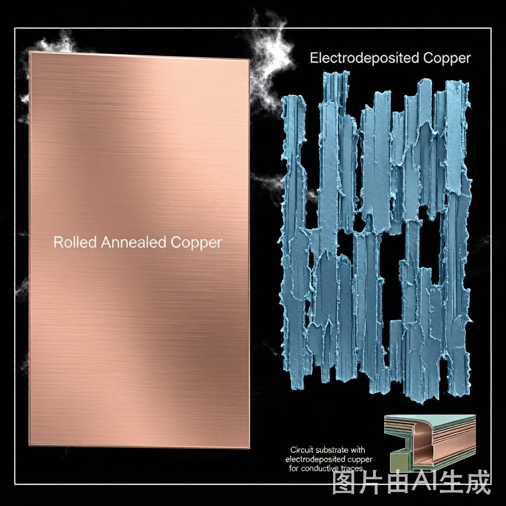
Electrodeposited (ED) Copper Foil
ED copper foil is manufactured by electroplating copper from a copper sulfate-sulfuric acid electrolyte onto a rotating titanium or stainless steel drum. Copper ions are reduced at the drum surface, building up a layer of pure copper that is continuously peeled off, washed, and wound onto rolls. Key characteristics:
- Grain shape: Columnar grains growing perpendicular to the drum surface; drum side is smooth, solution side has a rough, nodular topography
- Grain size: 0.1–5 μm, finer than RA foil
- Surface roughness (Ra): Drum side 0.1–0.3 μm (very smooth); solution side 1.5–8 μm (highly rough, optimized for dielectric adhesion)
- Thickness range: 9 μm to 105 μm; ultra-thin 5–6 μm grades available
- Purity: ≥99.8% copper
Bend Endurance: The Decisive Factor for Flexible Circuits
Bend endurance is where RA copper foil demonstrates its primary advantage. The lamellar grain structure of RA foil allows individual grains to slide past each other during bending, relieving stress without crack initiation. ED foil’s columnar grain boundaries, oriented perpendicular to the foil plane, act as crack initiation sites under cyclic bending.
| Parameter | RA Copper Foil | ED Copper Foil |
|---|---|---|
| Grain orientation | Parallel to foil plane (lamellar) | Columnar, perpendicular to plane |
| Bend cycles to failure (IPC-TM-650 2.4.3) | Typically 10×–100× greater than ED of same thickness | Lower; grain boundaries orthogonal to bend stress |
| Minimum bend radius | 3–6× foil thickness | 6–10× foil thickness |
| Dynamic flex life | Excellent; preferred for hinges, sliding mechanisms | Poor to fair; avoid in dynamic bend applications |
| Static bend stability | Excellent; low springback | Good; slightly higher springback |
For dynamic flex applications—foldable phone displays, printer head cables, robotic joint wiring—RA copper is the only reliable choice. For static bend applications where the circuit is bent once during assembly (e.g., co
ecting two rigid PCB sections in a rigid-flex design), ED copper can be acceptable when the bend radius is conservative.
Etch Quality and Fine-Pitch Capability
Copper foil etch behavior directly impacts the achievable trace width and spacing for fine-pitch SMT components. The fine, equiaxed grain structure of ED foil etches uniformly in all directions, producing clean trace edges with minimal undercut. RA foil’s larger, anisotropic grains can etch non-uniformly, with preferential attack along grain boundaries creating slightly serrated trace edges.
- ED advantage: Better etch uniformity; recommended for trace/space below 50 μm (2 mil)
- RA consideration: Acceptable for trace/space ≥75 μm (3 mil); diamond-like carbon (DLC) treatment of the matte side improves adhesion and etch uniformity for fine-pitch designs
- Surface treatment effect: Both foil types receive silane-based adhesion promoters and anti-tarnish coatings before lamination; these treatments minimally affect etch behavior
Signal Integrity at High Frequencies
At frequencies above 1 GHz, conductor surface roughness becomes a dominant contributor to insertion loss through the skin effect. Current concentrates in a thin layer at the conductor surface—the skin depth in copper at 5 GHz is approximately 0.93 μm. ED foil’s solution-side roughness (Ra 1.5–8 μm) effectively increases the conduction path length, raising insertion loss. RA foil’s inherently smoother surface (Ra 0.1–0.4 μm) provides lower insertion loss at high frequencies.
| Frequency | ED Foil Insertion Loss (dB/cm) | RA Foil Insertion Loss (dB/cm) |
|---|---|---|
| 1 GHz | 0.015–0.025 | 0.010–0.015 |
| 5 GHz | 0.035–0.060 | 0.020–0.030 |
| 10 GHz | 0.060–0.100 | 0.030–0.050 |
| 28 GHz (5G mmWave) | 0.120–0.200 | 0.060–0.090 |
For 5G mmWave (28 GHz+) and high-speed digital (PCIe 5.0, 32 GT/s NRZ) flexible circuits, RA copper foil with low-profile surface treatment is strongly recommended. Some manufacturers now offer “ultra-low-profile” ED foils with modified drum-side topography (Ra <0.5 μm) that approach RA foil insertion loss performance while maintaining ED's etch uniformity advantage.
Adhesion to Polyimide Dielectric
Polyimide adhesion strength is critical for fabrication yield and long-term reliability. ED foil’s high-roughness solution side provides excellent mechanical adhesion to cast polyimide, with typical peel strengths of 0.8–1.5 N/mm (IPC-TM-650 2.4.9). RA foil’s smoother surface produces lower raw peel strength (0.5–0.8 N/mm) but is routinely treated with copper oxide or silane coupling agents to achieve 0.7–1.2 N/mm—adequate for most applications including dynamic flex.
Cost and Availability Considerations
RA copper foil is generally more expensive than ED copper foil due to the mechanical rolling and a
ealing steps. For standard thicknesses (18 μm, 35 μm), RA foil carries a 20–50% cost premium. However, the cost differential narrows for ultra-thin foils (9–12 μm) and disappears for thicknesses below 9 μm, where ED is the only viable manufacturing process.
Selection Guide
| Application | Recommended Foil | Reason |
|---|---|---|
| Dynamic flex (hinge, sliding contact) | RA copper | Superior bend endurance |
| Static bend rigid-flex | RA or ED | Both acceptable; RA if bend radius is tight |
| High-speed digital (>5 GHz) | RA copper (low profile) | Lower insertion loss from skin effect |
| Fine-pitch (<50 μm L/S) | ED copper | Superior etch uniformity |
| Cost-sensitive consumer FPC | ED copper | Lower material cost |
| Aerospace / military FPC | RA copper | Maximum reliability margin |
Conclusion
The choice between RA and ED copper foil is rarely one-sided—it depends on the specific requirements of bend endurance, signal frequency, trace geometry, and cost targets. RA copper foil is the material of choice for dynamic flex and high-frequency applications where bend life and insertion loss are paramount. ED copper foil offers advantages in fine-pitch etching and cost for static or low-frequency flexible circuits. The most successful flexible PCB designs match the copper foil type to the most demanding requirement of the application, rather than defaulting to the cheapest or most familiar option.