The Mixed-Technology PCB Assembly Challenge
Many real-world electronic products combine surface mount (SMT) components with through-hole (THT) components on the same board—power supply boards with through-hole capacitors and inductors alongside surface mount ICs, automotive ECUs with through-hole co
ectors and large electrolytics, industrial control boards with through-hole relays and SMT microcontrollers. The challenge for SMT engineers is selecting the right soldering process to assemble both component types reliably on the same board without damaging either.
This guide examines the two dominant mixed-technology assembly approaches: conventional wave soldering with selective pallets, and selective wave soldering machines, comparing their process capabilities, thermal profiles, and economic tradeoffs.
Process Overview: Conventional Wave Soldering
Conventional wave soldering is a high-throughput process in which the entire bottom side of a PCB is passed over a wave of molten solder (typically SAC305 lead-free at 260–270°C) for 2–4 seconds. The solder wets all exposed metal surfaces on the bottom side, forming joints for through-hole pins and any bottom-side SMDs that are glued in place beforehand.
For mixed-technology boards, conventional wave soldering requires SMT components on the bottom side to be protected from the solder wave—either by:
- Selective (or palletized) wave soldering: A machined aluminum pallet masks the bottom-side SMT components, exposing only the through-hole areas to the wave
- Through-hole reflow (THR / Pin-in-Paste): Through-hole components are designed with through-hole terminations that can be soldered during the standard SMT reflow process, eliminating the wave step entirely. Requires precise solder paste printing in the through-holes and reflow-compatible component geometry.
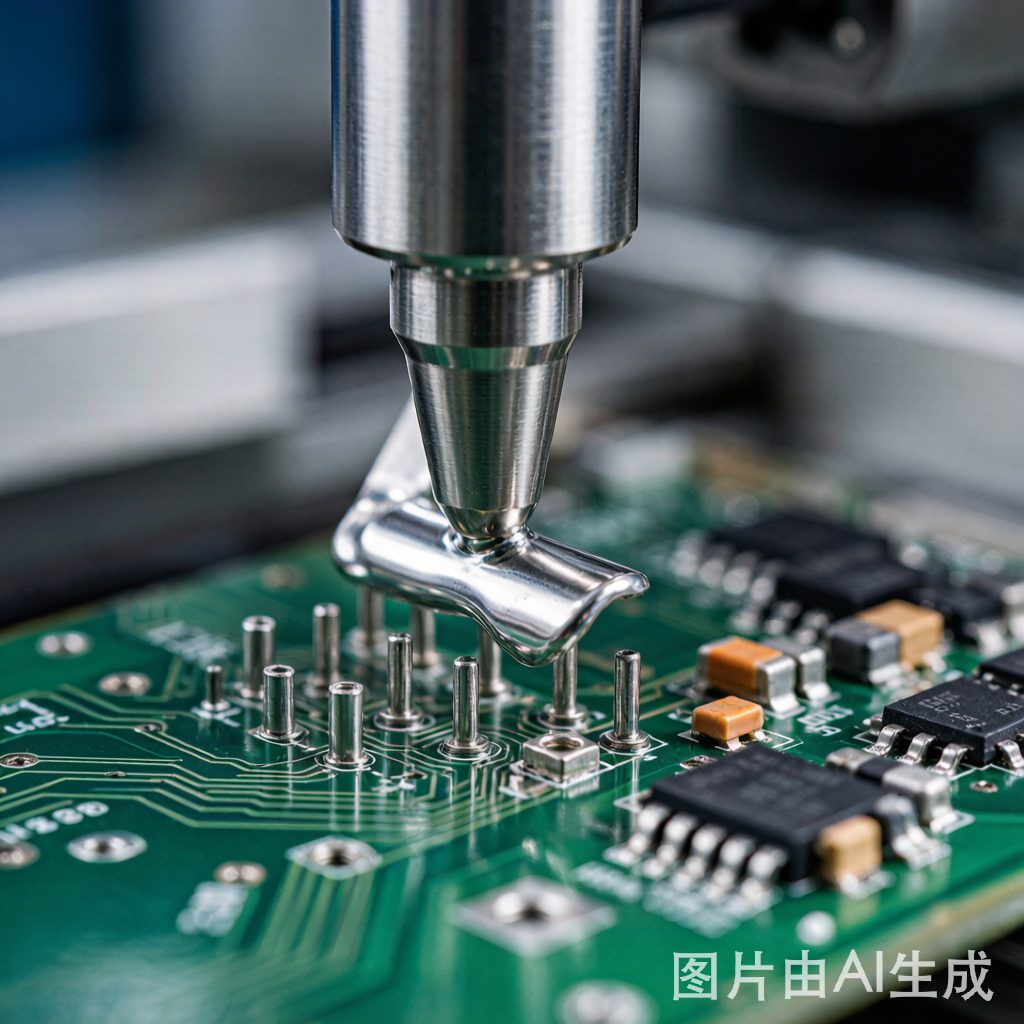
Process Overview: Selective Wave Soldering
Selective wave soldering uses a small, programmable solder nozzle (typically 3–30 mm diameter) mounted on an XYZ gantry system. The PCB is preheated to 100–140°C, then the nozzle dispenses a localized wave or jet of solder onto specific through-hole areas, one site at a time. Modern selective soldering machines handle 50–500+ solder joints per board with cycle times of 30–120 seconds.
Key process parameters include:
- Nozzle size and shape: Round nozzles (3–10 mm) for individual through-hole pins; elongated or custom-shaped nozzles (10–30 mm) for co
ectors and multiple-pin sites
- Solder pot temperature: 290–320°C for lead-free SAC305, higher than conventional wave due to localized application
- Dwell time: 1–4 seconds per joint, longer for high-thermal-mass through-hole components
- Preheating profile: Critical to drive off flux volatiles and reduce thermal shock; typically 100–140°C top-side preheat with controlled ramp
- Flux application: Spray flux is applied selectively only to through-hole sites, avoiding contamination of nearby SMT components
Thermal Comparison: Stress on SMT Components
Thermal stress is the primary differentiator between the two approaches:
| Process | Peak Board Temperature | Time Above 217°C | Thermal Stress on SMT |
|---|---|---|---|
| Conventional reflow (SAC305) | 240–250°C | 45–90 seconds | Baseline (full board, full profile) |
| Through-hole reflow (THR) | 240–250°C (same as SMT) | 45–90 seconds | Same as reflow; whole board sees one thermal cycle |
| Selective wave (localized) | 130–180°C on top side, 300°C+ locally at joint | 1–4 seconds per joint (cumulative much less than reflow) | Low; SMT components stay below 200°C |
| Conventional wave (with pallet) | 130–180°C on top side, 260–270°C on bottom | 2–4 seconds | Low on top; bottom-side SMT must be glued and pallet-protected |
Selective wave soldering’s localized application means SMT components on the same board experience much less thermal stress than they would in a full reflow cycle. This makes it ideal for temperature-sensitive components, large BGAs that have already been reflowed, and double-sided assemblies where one side has already been processed.
Joint Quality Comparison
Both processes produce acceptable through-hole joints when properly controlled, but with different characteristic qualities:
Through-Hole Joint Quality — Selective Wave
- Excellent hole fill for most through-hole components; typical 75–100% hole fill achieved
- Reduced thermal gradient across the board (controlled preheating)
- Less thermal shock on plated through-holes, particularly important for thick (>2.4 mm) PCBs
- Limited bridging and icicle defects due to localized flux application and no broad wave
Through-Hole Joint Quality — Conventional Wave
- Reliable hole fill for simple through-hole joints (co
ectors, axial components)
- Risk of insufficient hole fill for high-thermal-mass through-hole components (large transformers, ground planes) due to short wave contact time
- Higher bridging risk on closely-spaced through-hole pins without proper pallet masking
- Potential for solder skipping on heavily-plated ground areas that act as heat sinks
Through-Hole Reflow (Pin-in-Paste): The Alternative Approach
Through-hole reflow, also called pin-in-paste (PiP) or intrusive reflow, applies solder paste to through-holes during the SMT stencil printing step, then solders both SMT and through-hole components during the same reflow cycle. This approach eliminates the wave or selective soldering step entirely.
For successful pin-in-paste, the design must accommodate:
- Component geometry: Through-hole components must withstand standard reflow peak temperatures (240–250°C for SAC305) and have terminations that wick solder into the through-hole via capillary action
- Solder paste volume: Significantly more paste than SMT pads is required—typically 2–4× the hole volume to ensure complete hole fill after reflow. Stencil aperture design (often with secondary printing or step stencils) is critical.
- Component lead length: Lead protrusion on the solder side should be 0.5–1.5 mm to ensure proper wicking
- Plated through-hole design: Standard 25 μm copper plating and aspect ratio (board thickness / hole diameter) up to 2.5:1 are compatible with pin-in-paste
Pin-in-paste is often the most economical approach for high-volume mixed-technology boards because it eliminates secondary operations. However, it requires significant process development upfront and limits component selection to reflow-compatible through-hole parts.
Decision Framework: Which Process to Use
| Scenario | Recommended Process | Reason |
|---|---|---|
| High-volume consumer electronics with few THT | Pin-in-paste | Lowest cost, single reflow process |
| Industrial product with various THT sizes | Selective wave | Flexible, no stencil redesign, accommodates large THT |
| Power supply with large heat-sink and capacitors | Selective wave | High thermal mass, not suitable for reflow |
| Existing product with wave line and bottom-side SMT | Conventional wave + pallet | Leverages existing equipment investment |
| High-reliability aerospace/military with mixed tech | Selective wave | Process control, traceability per joint |
| Prototype / small batch mixed tech | Selective wave | Quick changeover, no stencil per board revision |
| Double-sided board, both sides already SMT | Selective wave | Through-hole add-on without disturbing SMT |
Equipment and Operating Cost Considerations
Selective wave soldering equipment represents a significant capital investment—$200,000–500,000+ for a production-scale system with dual solder pots, nitrogen atmosphere, and automated flux/board handling. By comparison, conventional wave soldering equipment starts at $50,000–100,000. Pin-in-paste requires only a standard SMT line with possibly a step-stencil modification, adding essentially no capital cost.
However, the operating cost analysis must consider throughput, changeover time, and defect rates:
- Selective wave: 30–120 seconds per board depending on joint count; low changeover time (program-driven); defect rates below 100–500 DPPM achievable with proper process control
- Conventional wave + pallet: 60–180 seconds per board including pallet loading/unloading; pallet design adds 1–3 days of upfront cost per board ($500–2,000 per pallet); defect rates 200–1,000 DPPM typical
- Pin-in-paste: 30–60 seconds per board on standard SMT line; very low changeover cost once stencil is designed; defect rates highly variable—200–2,000 DPPM depending on design discipline
For high-volume consumer products, pin-in-paste delivers the lowest cost per joint. For low-to-medium volume mixed-technology products, selective wave is typically the most cost-effective option once changeover flexibility is considered. For high-volume production of legacy mixed-technology boards, conventional wave with pallets remains competitive when pallet amortizes over many production runs.
Conclusion
Selective wave soldering and reflow-based pin-in-paste represent two distinct philosophies for mixed-technology PCB assembly, with conventional wave soldering as the legacy baseline. The best choice depends on production volume, design constraints, equipment investment, and the specific through-hole components involved. For products with substantial through-hole content or thermal-mass constraints, selective wave offers unmatched flexibility and joint quality. For high-volume designs with reflow-compatible through-hole components, pin-in-paste delivers the lowest total cost. The key engineering task is matching the process to the product’s design and manufacturing economics—not defaulting to familiar approaches when better alternatives exist.