Why PCB Stack-Up Design Is the Foundation of High-Speed Electronics
As digital signal speeds push into the multi-gigabit era—USB4 at 20 Gbps, 100 GbE Ethernet, PCIe 5.0 at 32 GT/s, and DDR5 at 6400 MT/s—controlled impedance interco
ects are no longer optional. The PCB stack-up design is the single most consequential decision in high-speed PCB engineering, dictating signal integrity performance, EMI behavior, power delivery quality, and manufacturing yield. A poorly conceived stack-up ca
ot be salvaged by careful routing; it imposes hard limits on every signal path that follows.
This guide walks through the practical engineering decisions behind a well-designed PCB stack-up, with emphasis on the materials, layer counts, and routing geometries most relevant to SMT manufacturing in commercial electronics.
Defining the Stack-Up Goals
Before selecting materials or layer counts, the stack-up must satisfy several often-competing requirements:
- Impedance control: Match characteristic impedance (typically 50 Ω single-ended, 85–100 Ω differential) for high-speed signals within ±10% tolerance
- Signal reference integrity: Provide a continuous return-current path adjacent to every signal layer
- Power distribution network (PDN) performance: Minimize power plane impedance at switching frequencies to suppress simultaneous switching noise (SSN)
- EMI control: Reduce common-mode radiation by containing high-speed signals between power/ground planes
- Manufacturability and cost: Use standard laminate thicknesses and avoid exotic materials when performance allows
Choosing the Layer Count
Layer count is driven by signal count, routing density, and signal integrity constraints. Common 2–10 layer stack-ups and their typical use cases:
| Layers | Typical Application | Routing Cha
els |
Cost Driver |
|---|---|---|---|
| 2 | Simple consumer products, low-speed MCU boards | 1 signal, 1 ground | Baseline cost |
| 4 | USB, HDMI, basic digital products | 2 signal + 2 plane | +30% over 2L |
| 6 | Ethernet, multi-rail power, moderate-speed SoC | 4 signal + 2 plane | +50% over 4L |
| 8 | DDR3/4, high-speed SoC, multi-gigabit SERDES | 6 signal + 2 plane | +35% over 6L |
| 10+ | PCIe Gen4/5, 100G networking, advanced ASICs | 8+ signal + 4+ plane | Premium tier |
A common 4-layer stack-up for moderate-speed designs places signals on the top layer, ground on layer 2, power on layer 3, and secondary signals on the bottom. This “Sig-GND-PWR-Sig” arrangement provides controlled-impedance microstrips on top and bottom layers with a clean return path on the adjacent ground plane. For high-speed designs, layer 2 is dedicated to high-speed signal routing, and a 6+ layer stack-up is used to ensure that each signal layer has a tightly coupled reference plane.
Microstrip vs Stripline Routing
Microstrip
Microstrip refers to a signal trace on an outer (top or bottom) layer with a single reference plane below it. The characteristic impedance is determined by trace width (W), trace thickness (T, typically 1 oz or 2 oz copper), and dielectric height (H) to the reference plane:
- Wider traces (4–8 mil for 50 Ω on 6-mil dielectric) are easier to manufacture but consume board area
- Microstrip exhibits faster propagation (≈150 ps/in on FR-4 εr=4.2) but more EMI radiation than stripline
- Best for moderate-speed signals up to 5 GHz where radiation is manageable
Stripline
Stripline routes the signal trace on an i
er layer sandwiched between two reference planes. The additional reference plane provides superior EMI containment and reduced crosstalk, at the cost of slower propagation (≈175 ps/in) and additional fabrication cost.
- Symmetrical stripline uses equal dielectric thicknesses above and below the trace, optimizing for clean return current splitting
- Asymmetric stripline (different dielectrics above/below) is common in cost-optimized stack-ups but requires careful via placement to maintain reference plane continuity
- Stripline is the standard for >5 GHz SERDES, high-speed backplanes, and EMI-sensitive applications
Dielectric Material Selection
Standard FR-4 (Tg 135–150°C, εr 4.2–4.5, Df 0.020) is the default choice for consumer and industrial electronics, but high-speed designs increasingly require low-loss materials:
| Material | εr @ 1 GHz | Loss Tangent | Typical Use |
|---|---|---|---|
| Standard FR-4 | 4.2–4.5 | 0.020 | < 5 Gbps, cost-sensitive |
| High-Tg FR-4 | 4.0–4.3 | 0.015 | Lead-free reflow + moderate speed |
| Mid-loss (e.g., Isola 408HR) | 3.7–3.9 | 0.012 | 5–10 Gbps, server/storage |
| Low-loss (e.g., Rogers RO4350B) | 3.48 | 0.0037 | 10–25 Gbps, RF/microwave |
| Ultra-low-loss (PTFE-based) | 2.2–3.0 | 0.001–0.002 | 28+ Gbps, mmWave, aerospace |
For 25 Gbps+ signaling, the loss tangent of FR-4 begins to dominate insertion loss, particularly for long trace lengths. Hybrid stack-ups that place the high-speed signals on Rogers RO4350B cores while using FR-4 subcomposites for power/ground and outer layers balance cost and performance.
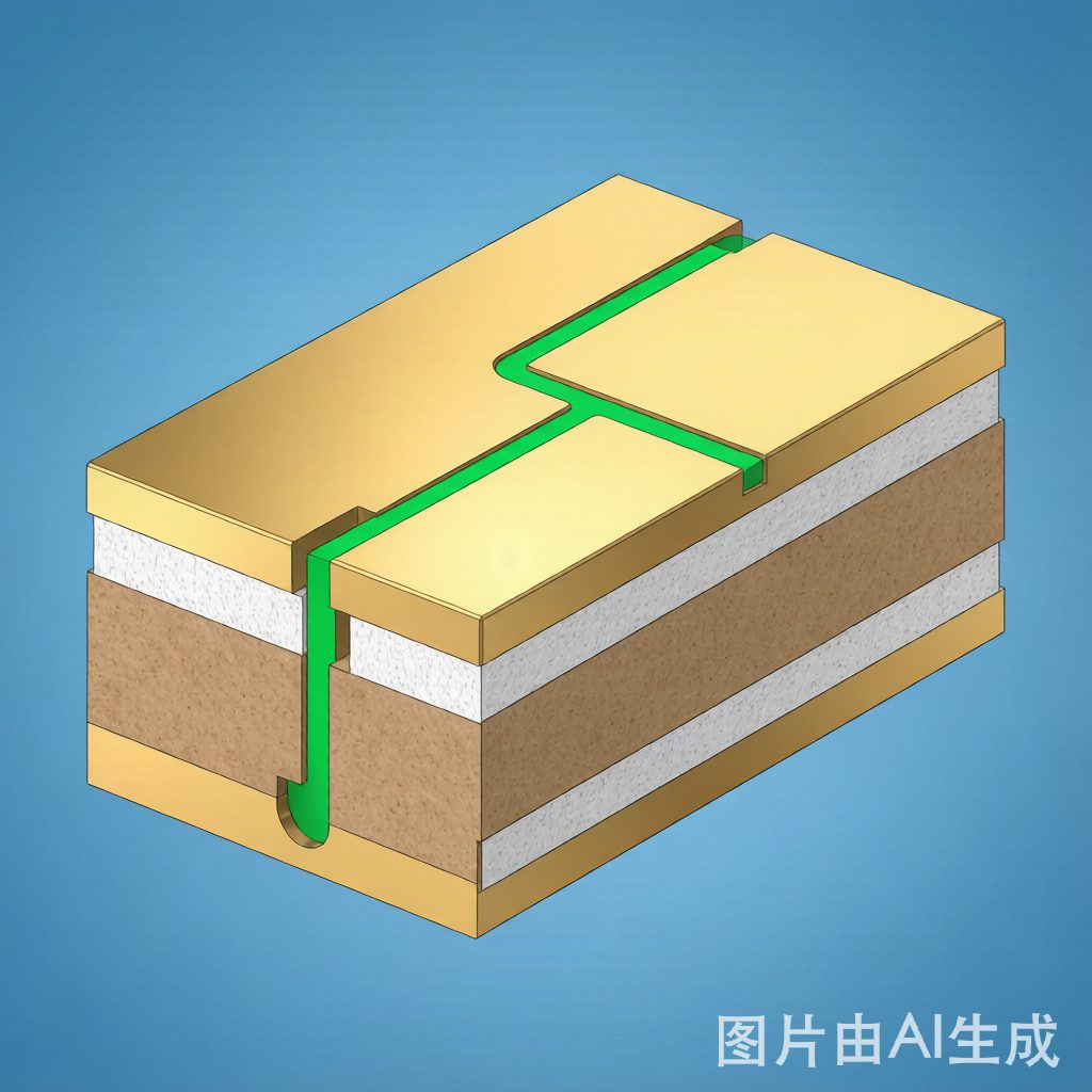
Prepreg and Core Selection
The dielectric between copper layers is built from a stack of prepreg (uncured fiberglass-epoxy sheets) and cores (cured laminates with copper bonded to both sides). Typical 6-mil prepregs (2116 or 1080 glass styles) and 8–12 mil cores provide the dielectric heights needed for 50 Ω microstrip on 4–6 mil traces. Standard prepreg styles are widely available, while exotic thin dielectrics (≤2 mil) drive cost and require tight process control at the PCB fabricator.
Critical stack-up rule: ensure at least one prepreg sheet between any signal layer and its reference plane, and use symmetric (mirror) construction around the board centerline to prevent warpage during lamination and reflow.
Power Plane and PDN Considerations
Power plane placement directly impacts PDN performance. The inductance of a power plane pair scales inversely with their spacing—a 4-mil power-ground spacing delivers approximately 1/3 the loop inductance of a 12-mil spacing. For high-current SMT components (FPGAs, SoCs with >10 A transient demands), placing the highest-current power rail on a plane pair tightly coupled to ground (≤6 mil) is critical for SSN suppression.
Decoupling capacitor placement must be optimized against plane inductance: 0402 capacitors with via-in-pad geometry (see our prior guide on VIP technology) deliver loop inductance below 0.5 nH, supporting effective decoupling at frequencies up to 1 GHz.
Manufacturing Cost Optimization
Stack-up decisions have direct cost implications. Strategies to balance performance and cost include:
- Use standard dielectric thicknesses: 4-mil, 6-mil, 8-mil, 12-mil cores and prepregs are widely available; exotic thicknesses drive custom process charges
- Minimize via types: A stack-up supporting both through and blind/buried vias is more expensive than a single-via design
- Limit material types: Mixing two material families (e.g., RO4350B + FR-4) is manageable; three or more materials compound fabrication complexity
- Symmetric construction: Mirror the stack-up to prevent warp and enable higher PCB panel yield
- Standard copper weights: 0.5 oz and 1 oz are mainstream; 2 oz or higher copper weight increases cost but enables high-current applications without busbars
Common Stack-Up Mistakes to Avoid
- Adjacent signal layers without a reference plane: Creates uncontrolled impedance and severe crosstalk
- Asymmetric construction: Causes warp during reflow soldering, leading to tombstoning and head-in-pillow defects during SMT
- Excessive thin-core stacking: 5+ thin cores in one board elevates fabrication cost and delamination risk
- Reference plane splits under high-speed signals: Return current must cross plane splits, creating EMI loops and signal integrity problems
- Ignoring Z-axis CTE: High layer count with standard FR-4 has z-axis CTE around 60 ppm/°C—risky for BGA components with fine pitch
Conclusion
A well-designed PCB stack-up is the structural foundation of any high-speed electronic product. Decisions about layer count, material selection, and routing geometry ripple through every subsequent design phase—from component placement to SMT manufacturing yield. The best stack-ups are the result of collaboration between electrical, mechanical, and PCB fabrication engineers, with the recognition that performance, manufacturability, and cost are simultaneously optimized. For products targeting 10+ Gbps signaling, investing in low-loss dielectric materials and a 6+ layer stack-up with tight power-ground coupling pays back many times over in field reliability and product performance.