What Is Via-in-Pad Technology?
Via-in-pad (VIP), also known as filled and capped via, is an advanced PCB fabrication technique where drilled vias are placed directly beneath surface mount component pads—rather than adjacent to them. This approach is a cornerstone of High-Density Interco
ect (HDI) PCB design, enabling the miniaturization demanded by modern electronics from smartphones to automotive ADAS modules.
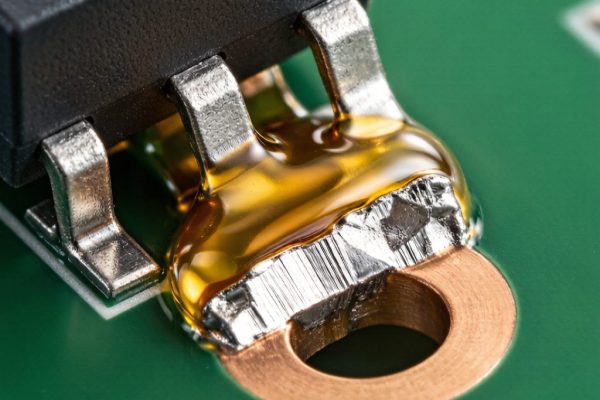
Traditional PCB design guidelines prohibit placing vias directly under component pads because unfilled vias cause solder to drain away during reflow, creating voids, cold joints, or component tombstoning. Via-in-pad resolves this by filling and capping vias before the outer copper layer is plated, creating a flat, solderable surface.
The Via-in-Pad Fabrication Process
Step 1: Via Drilling
Mechanical drilling (0.2–0.3 mm diameter) or laser drilling (0.075–0.15 mm for microvias) creates the through-holes or blind vias. Laser-drilled microvias are increasingly preferred for BGA pitches below 0.8 mm, where routing space is severely constrained.
Step 2: Copper Plating
Standard electroless copper seed layer deposition followed by electrolytic copper plating deposits copper on via barrel walls to IPC Class 2 or 3 standards (typically 25 μm minimum copper thickness in via barrel).
Step 3: Via Filling
The critical differentiator of VIP technology is how the via is filled. Common fill materials include:
- Conductive copper paste (electrolytic copper fill): Highest thermal and electrical conductivity; preferred for thermal vias under high-power components
- Non-conductive epoxy fill: Lower cost; adequate for signal vias where thermal performance isn’t critical
- Resin fill (thermally conductive): Middle-ground option with good thermal properties and lower cost than copper fill
Step 4: Planarization
After fill material curing, the via surface is mechanically planarized (back-grinding or belt sanding) to achieve a flat surface within ±12 μm across the pad area. This flatness is essential for reliable solder paste printing during SMT.
Step 5: Capping and Outer Layer Plating
A copper cap is electroplated over the planarized via, creating a continuous copper pad surface. The cap thickness is controlled to be flush with (or within 12 μm above/below) the surrounding copper plane.
Design Rules for Via-in-Pad
Implementing VIP requires adherence to specific design rules to ensure reliability:
- Via diameter: Maximum 0.25 mm for SMT pads; larger vias risk filling voids that cause solder joint issues
- Pad-to-via ratio: Via diameter should be no more than 50–60% of pad diameter to maintain adequate copper a
ular ring
- Copper fill grade: Specify IPC Type VII (copper-filled) for thermal vias under components with junction temperatures above 100°C
- Solder mask opening: Ensure solder mask openings align precisely with capped via pads; misregistration causes soldermask bridging
- Surface finish: ENIG (Electroless Nickel Immersion Gold) is strongly recommended over HASL for VIP pads due to ENIG’s flat surface profile
When to Use Via-in-Pad
Via-in-pad is justified when standard routing ca
ot accommodate required signal density or thermal performance:
- Fine-pitch BGA components (0.5 mm or 0.4 mm pitch): Escape routing requires vias directly in the BGA pad field
- QFN thermal pads: Large exposed pads on QFN/DFN packages require thermal vias for heat dissipation; VIP enables multiple vias under the pad without assembly issues
- High-speed differential pairs: Via-in-pad with controlled impedance minimizes stub length and reduces signal reflections at layer transitions
- Extreme miniaturization: IoT sensors, wearables, and medical implants where board area is severely constrained
Thermal Performance of Copper-Filled Via-in-Pad
For power electronics and LED driver PCBs, thermal via arrays under component pads are critical for heat extraction. Copper-filled VIP achieves thermal resistance of approximately 0.3–0.6°C/W per via (depending on via aspect ratio and fill quality), compared to 2–4°C/W for unfilled (air-filled) vias.
A typical design for a 5W power component might use a 5×5 array of 0.2 mm copper-filled VIP vias under a 3×3 mm thermal pad, providing approximately 0.05°C/W total thermal resistance through the via array—enabling efficient heat transfer to a backside copper plane or heatsink.
SMT Assembly Considerations for Via-in-Pad Boards
Via-in-pad boards require attention during SMT assembly:
- Solder paste volume: Slightly increase solder paste aperture (+5–10%) for VIP pads to compensate for any minor surface non-planarity
- Reflow profile: Standard SAC305 profile is compatible; ensure adequate soak zone to allow outgassing from epoxy-filled vias
- X-ray inspection: Post-reflow X-ray inspection is essential for BGA components on VIP boards to detect voids and confirm complete joint formation
- Voiding specification: IPC-7095 specifies maximum 25% void area for BGA joints; VIP with proper fill material typically achieves <10% voiding
Cost vs. Benefit Analysis
Via-in-pad adds 15–30% to PCB fabrication cost compared to standard HDI designs without VIP. However, the benefits often justify this premium:
- Enables smaller board form factors, reducing housing and mechanical costs
- Improved thermal management reduces heatsink requirements
- Higher signal integrity reduces EMI filtering component count
- Single board may replace multi-board assemblies in compact products
Conclusion
Via-in-pad technology is now a standard capability in advanced PCB fabrication for high-density, high-performance electronics. Understanding the fill material options, design rules, and assembly implications allows electronics engineers to leverage VIP effectively while managing cost and reliability tradeoffs. As component pitches continue to shrink with 0.3 mm BGA packages entering mainstream production, VIP will become increasingly indispensable in SMT circuit board design.