A QFN power amplifier dropping three watts or a BGA voltage regulator handling ten amperes must push its heat somewhere, and on a conventional multilayer board that destination is almost always an array of thermal vias directly beneath the exposed pad. Designed well, a via array cuts junction temperature by twenty to forty degrees Celsius; designed badly, it contributes almost nothing. This article walks through the numbers behind effective thermal via design.
The Heat Path Through a PCB
Heat generated at the die travels through the package paddle into the solder joint, then into a copper pad on the board surface. From there it must reach the internal copper planes, which are the only large thermal reservoirs on a typical board, and finally spread toward the board edges or a heatsink. The surface pad alone is tiny: a four-by-four-millimeter QFN paddle offers only sixteen square millimeters of copper, so without a path to the planes the pad saturates and the junction cooks.
Thermal vias are that path: short barrels of copper-plated fiberglass co
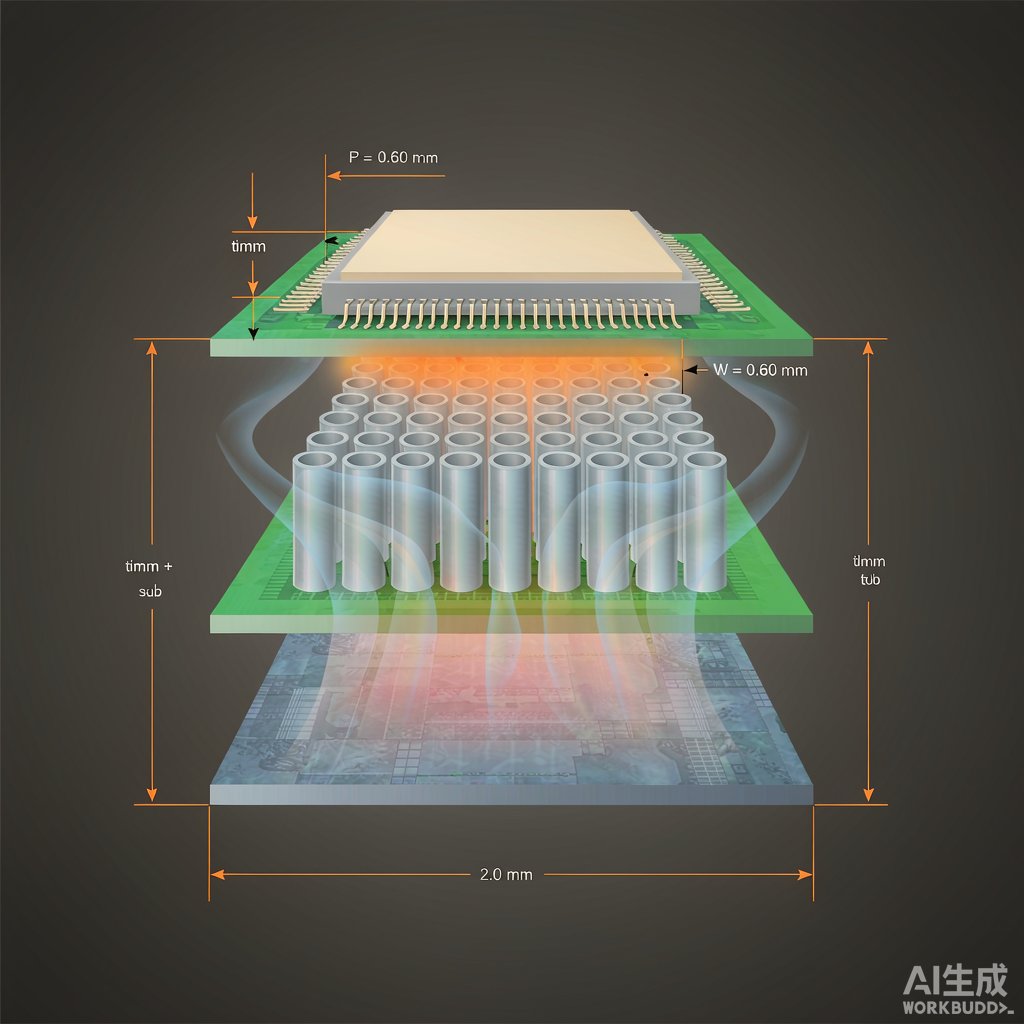
ecting the surface pad to one or more internal planes. Each via is a miniature heat conduit, and an array of them acts as a low-resistance bridge between the package and the thermal mass of the board.
Via Geometry: The Numbers That Matter
Drill Diameter and Plating Thickness
Thermal conductivity of a via is dominated by its copper cross-section. Standard practice uses 0.2 to 0.3 mm finished holes with 25 µm of plated copper walls. A single such via presents a thermal resistance on the order of one hundred kelvins per watt in isolation, which sounds useless until you remember that an array works in parallel: thirty-six vias drop the effective resistance to a few kelvins per watt.
- Small holes in dense arrays beat a few large holes: thermal resistance scales with hole length divided by copper area, and many short barrels outperform fewer fat ones once drilling cost is considered.
- Increasing plating from 25 µm to 50 µm roughly halves per-via resistance but consumes board-shop process margin; most designs reach their target with array size instead.
- Hole length matters: the same via array is roughly twice as effective in a 1.0 mm thick board as in a 2.0 mm one.
Copper Fill and Epoxy Fill
Solid copper-filled vias offer the lowest resistance but raise cost, so they are usually reserved for high-power or via-in-pad designs. Epoxy-filled and capped vias, classified as IPC-4761 Type VII, are the assembly-friendly standard for exposed-pad packages: the fill prevents solder from wicking down the barrel during reflow, and the copper cap lets the paddle solder directly over the array.
Array Layout Under the Package
Placement matters more than count. Distribute vias uniformly across the paddle footprint; concentrating them in the center leaves the corners of the solder joint hot and produces voiding at the edges. Typical arrays for a four-millimeter QFN use three-by-three to five-by-five patterns at 0.8 to 1.0 mm pitch, while a large BGA heat slug may take a seven-by-seven field or larger.
Pitch below about 0.8 mm starts to weaken the pad because the copper between holes loses mechanical continuity; pitch beyond 1.2 mm leaves dead zones in the middle of the joint. When the package datasheet supplies a recommended pattern, treat it as the starting point and adjust for your stackup and board thickness.
Co
ecting the Array to the Planes
An array tied to an internal plane through thermal-relief spokes can lose much of its advantage. Spokes thermally isolate a via on purpose, which is exactly what makes soldering possible on standalone ground pads. Under an exposed pad the goal is the opposite: co
ect every via to the plane with full, unbroken copper, and solve the soldering problem with the epoxy fill rather than with relief spokes.
Stackup synergy completes the design. Two-ounce outer copper on the top layer spreads heat laterally into the array, and at least one uninterrupted internal plane within 0.3 mm of the top surface gives the vias a short, wide landing. A classic four-layer stack with plane layers adjacent to both outer surfaces performs far better than the same copper area buried deep in an eight-layer board.
Assembly Pitfalls
- Solder wicking: unfilled vias under the paddle can swallow a large fraction of the printed paste, leaving voids or an open joint. Fill, cap, or tent vias before defining the paddle pad.
- Voids under the paddle: vias outgassing during reflow expand trapped air in the paddle joint. X-ray inspection routinely shows significant voiding on unoptimized layouts; keeping total void area below the IPC-A-610 Class 2 target usually requires via fill plus a windowpane aperture pattern in the stencil rather than one large opening.
- Keep-out errors: an anti-pad placed too close to the array islands the vias from the plane. Verify the actual copper in the layout database, not just the via symbols on the schematic.
Validating the Design
Simulation with a simple thermal resistance network or a field solver gives a first estimate, but the decisive test is empirical: attach a fine-gauge thermocouple on the paddle side of the board or use an infrared camera on a matte-black coated target, then compare the measured paddle temperature rise against prediction at full load. A well-designed array typically holds the paddle within five to ten degrees of the junction-side temperature; a twenty-degree delta signals that the path to the planes is broken somewhere.
Thermal vias are among the cheapest performance upgrades available in PCB design, adding no components and no assembly steps. The discipline lies in treating them as a designed feature with specified geometry, fill, and co
ection rules rather than an afterthought sprinkled under the package.