Introduction: Why Surface Roughness Matters on SMT Copper Strip
Surface-mount technology (SMT) copper strip is used for battery contacts, spring terminals, lead frames, bus bars, and shielding cans. While conductivity and alloy selection receive significant attention, surface roughness is equally critical because it controls how well the strip bonds to adhesives, accepts solder paste, and retains coatings. A surface that is too smooth can suffer adhesive delamination, while an overly rough surface can trap oxides, reduce solderability, and increase contact resistance.
Engineers working with stamped copper components must specify roughness parameters that balance mechanical interlocking with clean, wettable surfaces. This article explains the key roughness metrics for SMT copper strip, how they affect adhesive bonding and solderability, and practical process controls for achieving repeatable results.
Understanding Roughness Parameters: Ra, Rz, and Rmax
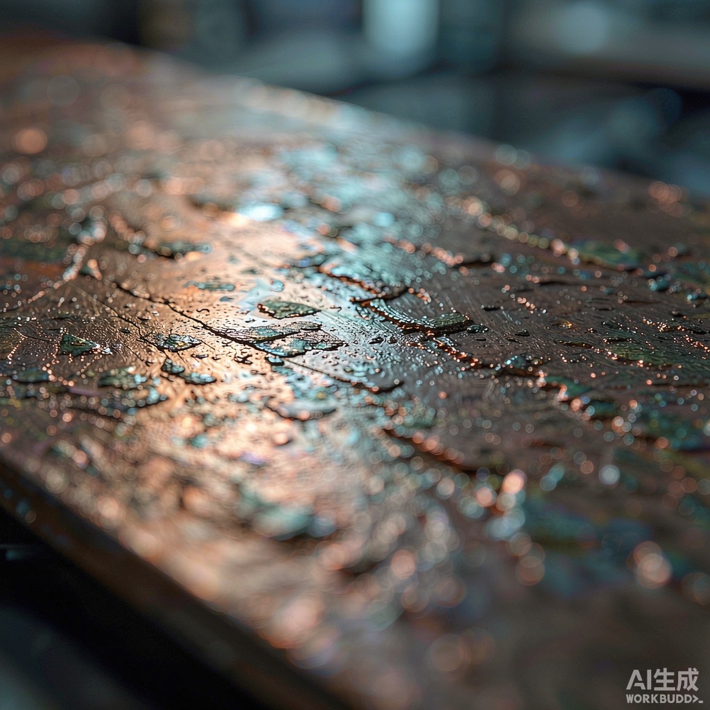
The most common roughness parameter is Ra, the arithmetic average deviation from the mean line over a sampling length. For SMT copper strip, Ra typically ranges from 0.1 µm for bright-a
ealed strip to 1.5 µm for as-rolled or specially textured strip. Ra is useful but does not capture peak-to-valley extremes, so engineers also use Rz, the average height difference between the five highest peaks and five deepest valleys within each sampling length. Rz is typically four to seven times larger than Ra for rolled copper.
Rmax reports the single largest peak-to-valley height in the evaluation length and is important when predicting coating thickness requirements or the risk of adhesive starvation at deep valleys. For fine-pitch SMT parts with pad pitches below 0.5 mm, Rmax should generally be kept below 6 µm to prevent solder paste bridging or inconsistent stencil release.
Effect of Roughness on Adhesive Bonding
Adhesives used in SMT assembly include conductive epoxies for die attach, thermally conductive acrylic tapes for LED modules, and structural adhesives for bonding copper terminals to plastic housings. Surface roughness influences adhesion through two competing mechanisms: mechanical interlocking and wetting.
For structural and conductive adhesives, moderate roughness improves bond strength by increasing the effective surface area and providing mechanical anchor points. An Ra between 0.4 µm and 1.2 µm often gives the best lap-shear strength with common epoxy and acrylic systems. Below 0.2 µm Ra, adhesives may not form sufficient mechanical interlock, especially after thermal cycling, leading to adhesive failure at the interface.
However, excessive roughness creates deep valleys that the adhesive ca
ot fully penetrate, trapping air and moisture. This is particularly problematic in tropical environments where humidity can migrate to the interface and accelerate corrosion. For copper strips bonded with conductive adhesives, an Rz above 8 µm can increase joint resistance and reduce long-term reliability. Plasma or corona treatment can improve wetting without changing roughness dramatically.
Effect of Roughness on Solder Paste Transfer and Reflow
Solder paste stencil printing depends on consistent paste release from the stencil aperture onto the copper pad or strip. Surface roughness affects both the volume of paste deposited and the uniformity of paste spread after printing. On very smooth surfaces with Ra below 0.15 µm, solder paste can slump or spread beyond the pad boundary, increasing the risk of bridging during reflow. On very rough surfaces, paste can be retained in surface valleys, reducing the effective paste height and causing insufficient solder joints.
Industry experience suggests an Ra range of 0.3 µm to 0.8 µm provides good solder paste release and reflow wetting for SAC305 and Sn100C alloys. For immersion tin or nickel-palladium-gold finished copper strip, the plating process usually produces smoother surfaces, so stencil aperture design should be adjusted to compensate. Pre-ti
ing or reflow tin plating can also smooth sharp asperities while improving solderability.
Process Control and Measurement
Roughness should be measured with a contact profilometer or optical 3D profiler at multiple locations along the strip width and length. Variations across the coil can indicate roll wear, lubricant breakdown, or uneven tension. Standard sampling plans might measure Ra, Rz, and Rmax every 500 meters for high-volume production.
Process levers for adjusting roughness include:
- Cold rolling: Smooths the surface; successive passes reduce Ra.
- Skin pass: A light cold-rolling pass that sets final roughness and flatness.
- Brushing or polishing: Reduces peak height selectively for solderability-critical applications.
- Texturing: Controlled roughening for adhesive bonding applications.
Recommended Roughness Targets by Application
For SMT copper strip used in soldered contacts, target Ra 0.3–0.6 µm, Rz 2–4 µm, and Rmax below 5 µm. For adhesive-bonded terminals, target Ra 0.5–1.2 µm, Rz 3–7 µm, and Rmax below 8 µm. For plated strip, ensure the base roughness is compatible with the pla
ed plating thickness; thin finishes below 1 µm may not fill deep valleys.
Conclusion
Surface roughness on SMT copper strip is a hidden variable that strongly influences adhesive bonding, solder paste transfer, coating adhesion, and long-term reliability. By specifying the right Ra, Rz, and Rmax ranges for each application and monitoring roughness during production, manufacturers can reduce defects, improve first-pass yield, and build more durable electronic assemblies.