Why PEEK in Semiconductor Fixturing
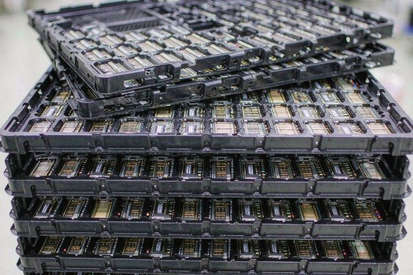
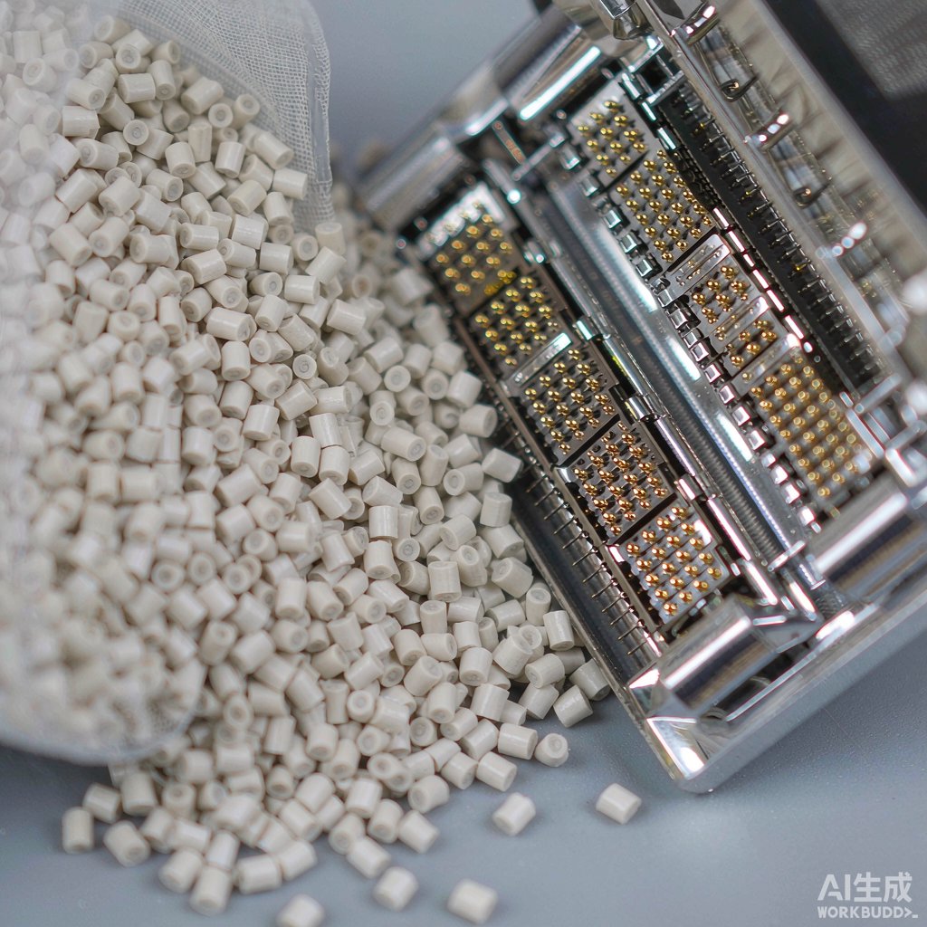
Semiconductor test sockets and wafer handling tools operate in some of the most demanding conditions in plastics processing. They must endure repeated thermal cycling, maintain tight dimensional tolerances, resist wear from contact insertion, and often dissipate static charge. Polyetheretherketone (PEEK) plastic pellets have become the material of choice for these precision components.
PEEK is a high-performance semi-crystalline thermoplastic with a glass transition temperature near 143°C and a melting point around 343°C. Its combination of thermal stability, mechanical strength, and chemical resistance makes it far more durable than standard engineering plastics like POM or PA66 in wafer-test environments.
Key Properties of PEEK Pellets
Thermal Stability
PEEK retains mechanical properties up to 250°C continuous use temperature. This allows test sockets to survive burn-in boards and high-temperature probe tests where devices are exercised at 150°C or above. Crystallinity control during injection molding is critical; under-crystallized parts soften earlier, while over-crystallized parts become brittle.
Dimensional Precision and Creep Resistance
Test socket holes and contact cavities must remain within ±10 µm over thousands of insertion cycles. PEEK offers low creep and excellent elastic recovery compared to most thermoplastics. Filled grades with 30% glass fiber or carbon fiber further reduce thermal expansion and improve stiffness, although they increase tool wear during machining.
Chemical and Wear Resistance
PEEK resists acids, bases, and solvents used in wafer cleaning processes. For test sockets with high insertion cycles, carbon-fiber or PTFE-modified PEEK grades reduce friction and extend socket life. Hardness can be tuned between 80 and 90 Shore D depending on filler selection.
ESD and Conductive Grades
Static discharge can destroy delicate dies during wafer handling. Conductive PEEK pellets compounded with carbon nanotubes, carbon fiber, or graphite provide surface resistivity in the 104–109 Ω/sq range. These ESD-safe grades prevent charge accumulation while maintaining most of PEEK’s mechanical and thermal properties.
Processing Guidelines
Drying and Molding
PEEK pellets must be dried at 150°C for 3–4 hours to reduce moisture below 0.02%. Barrel temperatures range from 360°C to 400°C, and mold temperatures of 160–200°C promote proper crystallization. Shear-sensitive fillers require moderate screw speeds to prevent fiber breakage.
Machining and Finishing
Many test sockets are injection molded near-net-shape and then machined to final tolerances. Sharp carbide tools, moderate feed rates, and coolant suitable for high-temperature polymers produce the best surface finish. A
ealing after machining relieves residual stress and improves long-term dimensional stability.
Conclusion
PEEK plastic pellets provide the thermal, mechanical, and electrical properties required for semiconductor test sockets and wafer handling. Selecting the right grade and controlling crystallinity during processing ensures reliable performance in high-temperature, high-precision test environments.