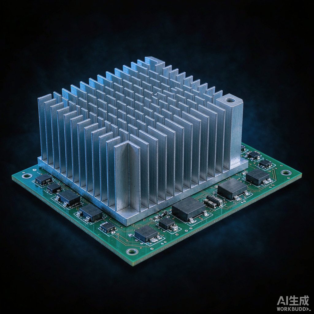
Power-dense SMD parts — LDO regulators, DC-DC modules, MOSFETs, LED drivers, gate drivers — routinely hit junction temperature limits on layouts that looked fine in the schematic. When board-level copper spreading is not enough, a heat sink on top of the package is the next tool. This guide covers how to size one, choose the fin geometry, attach it properly, and avoid the mistakes that make heat sinks ineffective.
Start With the Thermal Budget
Before browsing catalogs, compute the required thermal resistance:
θ_required = (T_j,max − T_ambient) / P
Example: a MOSFET dissipating 3 W with T_j,max = 125 °C in a 60 °C enclosure gives a budget of about 21.7 °C/W for the entire junction-to-ambient path. Compare that with the datasheet θ_JA (often 40–80 °C/W for SMD packages) and you can see immediately how much resistance the sink plus interface must remove.
Reading Datasheet Thermal Metrics Correctly
- θ_JA is measured on standardized JEDEC JESD51 boards in still air. Your board has different copper area and airflow, so treat θ_JA as a comparison number between packages, not a prediction.
- θ_JC (top) describes the resistance from junction to the top of the package case — this is the number to pair with a top-mounted heat sink. If θ_JC is large (small or plastic-lidded packages), a heat sink helps little because the bottleneck is inside the package.
- θ_JB / Ψ_JT help estimate junction temperature from a case or board temperature measurement during validation.
Heat Sink Sizing Basics
Natural Convection Limits
In still air, flat surfaces transfer roughly 5–10 W/m²·K. A natural-convection sink needs surface area — usually achieved with fins — and the classic rule is fin spacing of 6–10 mm for vertical fins in free air. Pack fins tighter than that and boundary layers merge, so added fins stop adding cooling.
Fin Orientation and Airflow
Fins work best when air can flow through them vertically (chimney effect) or along them in forced flow. A fin stack mounted horizontally with fins facing the ceiling can lose 20–30% of its rated performance. Match the sink’s rated airflow direction to how your product will actually stand or hang.
Material and Process
- Extruded aluminum (6063) is the default: cheap, good fin aspect ratios up to about 10:1.
- Stamped sinks suit low-power, high-volume SMD cooling where cost rules.
- Skived, bonded, or forged fins reach higher density for forced-air, space-limited designs.
- Copper sinks double thermal conductivity but triple weight and cost — reserve for hot spots with severe constraints.
Attachment Methods and Interface Materials
The sink-to-case joint is where most installations fail. Every interface adds resistance; a dry joint can contribute more θ than the sink itself.
- Thermal adhesive or epoxy: Permanent, no mechanical retention needed. Choose a gap-filling grade with 1–3 W/m·K for irregular SMD topsides. Watch out for rework — epoxy usually destroys the part on removal.
- Spring clips: The best choice for plastic SMD packages. Clips apply controlled pressure without stressing the package and allow rework, but need board anchors or plastic pins.
- Screws through the board: Only for packages with proper mounting holes; follow the datasheet torque sequence to avoid cracking the mold compound.
Choosing the Thermal Interface Material
Gap pads suit the 0.2–2 mm tolerance stack over SMD bodies; pick a soft, high-conformance material and specify thickness so compression lands around 20–30%. Thermal grease gives the lowest resistance for flat metal lids but pumps out under thermal cycling on clip-less assemblies. Whatever you choose, the joint pressure and gap tolerance must be measured on the actual assembly, not assumed from CAD.
Common Design Mistakes
- Ignoring the board path: On packages whose main heat exit is downward (paddle packages), a top sink can be theater. Improve pads, vias, and internal planes first, or use a sink on the PCB underside.
- Blocking airflow: Tall fin stacks squeezed between neighboring capacitors stall the air. Check clearances in the mechanical model.
- Sealed enclosures: A sink inside a closed plastic box just moves heat from the chip to the enclosure air. Provide vents or conduct the heat to the housing wall.
- Forgetting radiation: In natural convection products, anodized or painted sinks radiate measurably better than bright bare aluminum — often worth 5–10% in a cool enclosure.
Verifying the Result
Prototype validation closes the loop. Attach a fine-gauge thermocouple (36–40 AWG) to the case with thermal epoxy and log temperature at steady state, then back-calculate junction temperature using Ψ_JT. Infrared cameras help find surprises, but shiny metal tops need a dab of matte tape or paint for accurate readings. Finally, run a power-cycling test — joints and TIMs age, and the failure mode you care about is temperature drift over thousands of cycles.
Conclusion
Effective SMD heat sinking is arithmetic first and hardware second. Derive the resistance budget from junction limit, ambient, and dissipation; confirm the package’s heat actually exits through the top; select fin geometry matched to real airflow; and engineer the attachment as carefully as the sink. A modest, well-mounted clip-on sink with the right interface material will outperform a large sink glued on as an afterthought every time.