## The Critical Role of Solder Retention in EMI Shielding
An EMI shielding can is only as effective as the mechanical and electrical integrity of its solder attachment to the PCB. Poor solder retention leads to shield lift during thermal cycling, degraded grounding continuity, and ultimately failed EMC compliance. This article covers the design rules that ensure reliable solder joints between shielding cans and PCB land patterns.
## Understanding EMI Shielding Can Types
### Two-Piece Shielding Systems
Two-piece shielding systems consist of a stamped metal fence (frame) and a removable lid (can). The frame is soldered to the PCB during reflow, and the lid snaps onto the frame after assembly. This design allows access to components under the shield for rework.
Solder retention in two-piece systems focuses on the frame-to-PCB interface, which has a continuous solder joint along the fence perimeter.
### One-Piece Shielding Cans
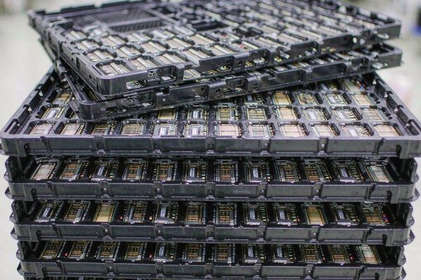
One-piece cans combine the fence and lid into a single stamped component. They are placed onto pre-applied solder paste and reflowed in the same pass as other SMT components. One-piece cans are simpler to assemble but ca
ot be removed for rework without desoldering.
## Land Pattern Design for Maximum Solder Retention
### Land Width and Length
The PCB land pattern for a shielding can fence should extend 0.3–0.5 mm beyond the fence footprint on each side. This creates a solder fillet that mechanically anchors the fence to the land.
For a 0.40 mm wide fence, the recommended land width is 1.0–1.2 mm. The extra width provides:
– A fillet area for mechanical strength
– A solder paste deposition zone
– A tolerance margin for placement accuracy
### Land Geometry for Corners
At shield corners where two fence sections meet, the land pattern should include a pad extension or thermal relief to prevent solder starvation at the corner. A common approach is to increase the corner land area by 50% compared to straight sections, ensuring adequate paste volume at the corner junction.
### Via-in-Pad Considerations
When grounding vias must be placed within the shield land area, via-in-pad design with plating and filling is required to prevent solder wicking into the via and reducing available paste volume at the joint.
If via-in-pad is not feasible, vias should be placed outside the land area and co
ected with a short trace. This adds a small amount of inductance to the ground path but preserves solder joint integrity.
## Stencil Aperture Design
### Aperture Dimensions
The stencil aperture for a shielding can should be 0.05–0.10 mm smaller than the PCB land on each side. This prevents paste from extending beyond the land onto the solder mask, which can cause solder balls during reflow.
For a 1.0 mm wide land, the aperture width should be 0.80–0.90 mm.
### Aperture Thickness
Standard SMT stencil thickness is 0.12–0.15 mm. For shielding cans, this is generally sufficient because the joint does not require large paste volumes. However, for tall shields (height > 5 mm) or heavy shields (weight > 5 grams), consider increasing local stencil thickness using a step-up stencil to provide additional paste for mechanical strength.
### Multi-Print Stenciling
For applications requiring very high solder joint reliability (automotive, aerospace), a multi-print approach can be used: print a standard layer, then overprint a second layer with a smaller aperture. This doubles the paste volume in the joint area and creates a larger fillet, significantly improving mechanical retention.
## Reflow Profile Considerations
### Thermal Mass Disparity
Shielding cans have significantly more thermal mass than typical SMT components (resistors, capacitors, IC packages). This means they reach reflow temperature later in the profile. If the profile is optimized for smaller components, the shield joint may not fully reflow, resulting in cold solder joints and poor retention.
### Profile Adjustment Strategy
To accommodate the thermal mass of shielding cans:
1. Extend soak time by 20–30 seconds to allow the shield to approach reflow temperature gradually
2. Increase peak temperature by 5–10°C above the standard profile (ensure this is still within the solder paste manufacturer’s specifications and component temperature limits)
3. Verify with thermocouples attached to the shield surface and the PCB land to confirm actual reflow temperature is achieved at the joint interface
### Nitrogen Reflow
Nitrogen-assisted reflow (oxygen levels < 1000 ppm) improves solder wetting on tin-plated shield fences, creating a more uniform fillet and stronger mechanical joint. For lead-free SAC305 solder, nitrogen reflow is particularly beneficial because the higher surface tension of SAC alloys makes wetting more sensitive to surface oxidation.
## Shield Placement Accuracy Requirements
Shielding cans require placement accuracy of ±0.15 mm or better. Misalignment beyond this tolerance creates:
– Uneven solder fillets (one side thick, opposite side starved)
– Reduced mechanical strength on the thin-fillet side
– Potential contact between the shield fence and adjacent component pads
For manual placement or older pick-and-place equipment, consider using fiducial marks on the shield land pattern to improve placement accuracy.
## Mechanical Design Factors Affecting Retention
### Fence Thickness
Standard shielding can fence thickness is 0.20–0.30 mm. Thi
er fences (0.15 mm) are easier to form but provide less mechanical strength at the solder joint. Thicker fences (0.30–0.40 mm) improve retention but require more force during placement and may cause PCB warpage.
### Tin Plating Quality
The tin plating on the shield fence directly affects solderability. Matte tin plating (3–5 µm) is standard for shielding cans. Insufficient plating thickness or oxidation of the tin surface creates wetting problems that reduce solder joint strength.
### Shield Flatness
The bottom edge of the fence (the surface that contacts the PCB land) must be flat within 0.05 mm. Shield cans that are not flat after stamping create gaps that allow solder to flow unevenly, creating weak joints on one side and solder bridges on the other.
## Testing Solder Retention
### Mechanical Pull Test
The most direct test for solder retention is a mechanical pull test: apply an upward force to the shield at a controlled rate (typically 5–10 mm/min) and measure the force at which the solder joints fail. Acceptable pull strength depends on shield size but should be at least 50% of the theoretical joint shear strength.
### Thermal Cycling Test
Thermal cycling from -40°C to +125°C for 500–1,000 cycles reveals solder joint fatigue. After cycling, shields should pass both pull testing and visual inspection for solder cracks.
### Cross-Section Analysis
Cross-sectioning the solder joint and examining under magnification reveals:
– Fillet shape and height
– Intermetallic compound layer thickness (target: 1–4 µm for SAC305)
– Voids within the joint
– Cold joint indicators
## Common Failure Modes and Prevention
### Solder Starvation at Corners
Corner joints are the most common failure point. Prevention: enlarge corner land areas and verify paste deposition at corners during stencil optimization.
### Tombstoning During Reflow
Small shields with asymmetric thermal mass can tombstone (tilt during reflow). Prevention: balance paste volume on opposing sides and ensure the reflow profile has a gentle ramp rate through the liquidus temperature.
### Shield Lift After Thermal Cycling
Differential thermal expansion between the shield (typically tin-plated steel or copper alloy) and the PCB (FR-4 or high-Tg laminate) creates shear stress on the solder joints. Prevention: use a flexible solder paste formulation or design mechanical retention features (clips, tabs) in addition to the solder joint.
## Conclusion
Reliable EMI shielding can solder retention requires attention to land pattern design, stencil aperture optimization, reflow profile adjustment for thermal mass, and verification through mechanical testing. By following these design rules, electronics manufacturers can achieve shielding cans that maintain both EMC performance and mechanical integrity throughout the product lifetime. TechMartSE supplies tin-plated shielding cans and fencing materials suitable for SMT assembly, with customizable dimensions and plating specifications.