## Introduction
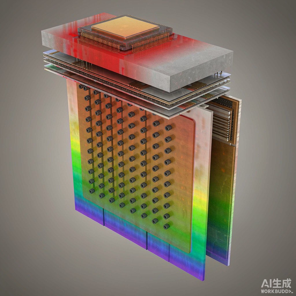
As power density in SMT electronics continues to climb — driven by 5G power amplifiers, EV charging controllers, and high-brightness LED arrays — conventional FR-4 PCBs struggle to dissipate heat fast enough to keep junction temperatures within safe operating limits. One solution gaining traction in tropical and high-ambient environments is the embedded copper core PCB, where a solid copper inlay or thick copper plane is integrated into the PCB stackup to create a low-resistance thermal path from the heat-generating component to the ambient.
This article provides a practical thermal resistance modeling framework for embedded copper core designs, comparing inlay versus laminated approaches and offering material selection guidance for SMT applications operating in ambient temperatures of 35–45 degrees Celsius.
## Thermal Resistance Network Fundamentals
### The Junction-to-Ambient Pathway
Total thermal resistance from junction to ambient (RthJA) is the sum of several series and parallel resistances:
1. Junction-to-case (RthJC): determined by the semiconductor package design, typically 1–5 degrees C per watt for power devices.
2. Case-to-copper core (RthCC): the interface resistance between the component package and the embedded copper, including solder or thermal adhesive layers.
3. Copper core spreading resistance (Rthspread): the resistance to heat spreading laterally within the copper inlay, which is a function of copper thickness, area, and thermal conductivity (400 W/m·K for pure copper).
4. Copper-to-ambient (RthCA): the final convective and radiative heat transfer from the PCB surface to ambient air.
### Spreading Resistance: The Dominant Term
In most embedded copper core designs, spreading resistance within the copper is the dominant thermal resistance. For a circular heat source of radius r on a copper disc of radius R and thickness t, the spreading resistance can be approximated:
Rthspread = (1 / (4 pi k r)) (1 – (r / R)) * (1 + ln(R / r))
where k is copper thermal conductivity. For a typical SMT power device with a 3 mm x 3 mm thermal pad on a 20 mm x 20 mm copper inlay of 1.0 mm thickness, Rthspread is approximately 2.5–3.5 degrees C per watt. Doubling the inlay thickness reduces spreading resistance by approximately 30%.
## Inlay Versus Laminated Copper Core Designs
### Copper Inlay (Embedded Solid Copper)
In this approach, a solid copper piece is machined and inserted into a routed cavity in the FR-4 PCB during fabrication. The copper is bonded to the surrounding FR-4 using a high-thermal-conductivity adhesive (typically 1–5 W/m·K epoxy). The advantage is excellent thermal performance — the copper can be 1–3 mm thick, providing superior heat spreading. The disadvantage is added manufacturing complexity and cost, as the PCB requires routing and insertion steps.
### Thick Copper Laminate (Heavy Copper PCB)
In this approach, a thick copper layer (typically 3–10 oz, or 105–350 micrometers) is laminated as part of the standard PCB stackup. This is simpler to manufacture but provides less copper thickness than an inlay. For a 4 oz copper (140 micrometers) layer, the thermal spreading is adequate for devices dissipating 2–5 watts but insufficient for devices above 10 watts.
### Comparison Table
| Parameter | Copper Inlay | Heavy Copper Laminate |
|—|—|—|
| Copper thickness | 1–3 mm | 0.1–0.35 mm |
| Spreading resistance (3 mm source) | 2–4 C/W | 8–15 C/W |
| Manufacturing complexity | High (routing + insertion) | Moderate (standard PCB process) |
| Cost premium over FR-4 | 40–80% | 15–30% |
| Suitable power dissipation | 10–50 W | 2–10 W |
| Thermal interface to component | Direct solder to copper | Through copper plane |
## Material Selection for Tropical High-Ambient Applications
### Ambient Temperature Derating
In tropical climates where ambient temperatures reach 35–45 degrees Celsius, the available temperature budget for component temperature rise is reduced. A component with a maximum junction temperature of 150 degrees C has only 105–115 degrees C of rise available (versus 120–125 degrees C in a 25-degree controlled environment). This 10–20 degree reduction in thermal budget must be compensated by improving the copper core thermal path.
### Copper Purity and Thermal Conductivity
The thermal conductivity of copper used in PCB cores varies with purity and temper:
– C11000 (ETP copper): 390 W/m·K — standard electronic grade, readily available.
– C10200 (OFHC): 400 W/m·K — oxygen-free, marginal improvement, higher cost.
– C19400 (CuFe2P): 260–300 W/m·K — used for leadframes, lower conductivity but better mechanical strength.
For pure heat spreading applications, C11000 offers the best balance of conductivity and cost. The 2–3% conductivity advantage of OFHC is rarely worth the 30–50% cost premium.
### Thermal Interface Material Between Component and Copper Core
The interface between the SMT component and the embedded copper is critical. Options include:
– Solder (SAC305): thermal conductivity 58 W/m·K, bond line thickness 25–75 micrometers, giving Rth of 0.04–0.13 C/W. Best for permanent attachments.
– Thermal grease: 3–8 W/m·K, bond line 25–50 micrometers, Rth 0.5–1.7 C/W. Used for serviceable attachments.
– Phase change material: 4–6 W/m·K, bond line 15–30 micrometers, Rth 0.25–0.75 C/W. Good compromise between performance and reworkability.
## Thermal Vias: Bridging Layers to the Copper Core
### Via Design Rules
When the heat source is on the outer PCB layer and the copper core is embedded in an i
er layer, thermal vias create the co
ection. Recommended design rules:
– Via diameter: 0.2–0.3 mm (plugged with copper or thermally conductive fill).
– Via pitch: 0.5–0.8 mm in a staggered array beneath the thermal pad.
– Array size: extend 1–2 rows beyond the component thermal pad footprint.
– Plating: 25–35 micrometers copper, optionally capped with copper to eliminate air voids.
Each thermal via has a thermal resistance of approximately 5–10 C/W per via. A 5×5 via array reduces the effective resistance to 0.2–0.4 C/W, which is negligible compared to spreading resistance.
## Practical Case Study: 350W EV Charging Control Module
Consider an EV charging control module with two MOSFETs each dissipating 8 watts, mounted on a 40 mm x 60 mm PCB with a 1.5 mm thick copper inlay. The ambient temperature is 40 degrees C (tropical outdoor enclosure).
– RthJC: 1.5 C/W per MOSFET.
– Rth (solder interface): 0.08 C/W.
– Rth (spreading in 1.5 mm copper): 2.8 C/W (calculated using the circular source approximation).
– Rth (copper-to-ambient, natural convection): 12 C/W.
Total RthJA: 1.5 + 0.08 + 2.8 + 12 = 16.4 C/W.
Junction temperature rise: 8 W x 16.4 = 131 degrees C.
Junction temperature: 40 + 131 = 171 degrees C — exceeding the 150 degrees C limit.
This calculation shows that even with an embedded copper core, natural convection is insufficient. Adding a small 40 mm fan to reduce RthCA from 12 to 4 C/W brings the junction temperature to 40 + 8 x (1.5 + 0.08 + 2.8 + 4) = 40 + 67 = 107 degrees C — well within limits.
## Conclusion
Embedded copper core PCBs are a powerful thermal management tool for high-power SMT electronics, but their effectiveness depends on careful thermal resistance modeling. The dominant resistance is often spreading within the copper, which can be reduced by increasing inlay thickness and area. In tropical environments with high ambient temperatures, active cooling (fans or heat sinks) is frequently necessary to supplement the copper core’s passive spreading capability. By following the modeling approach and material selection guidance in this article, engineers can design copper core PCBs that reliably keep junction temperatures within safe limits.