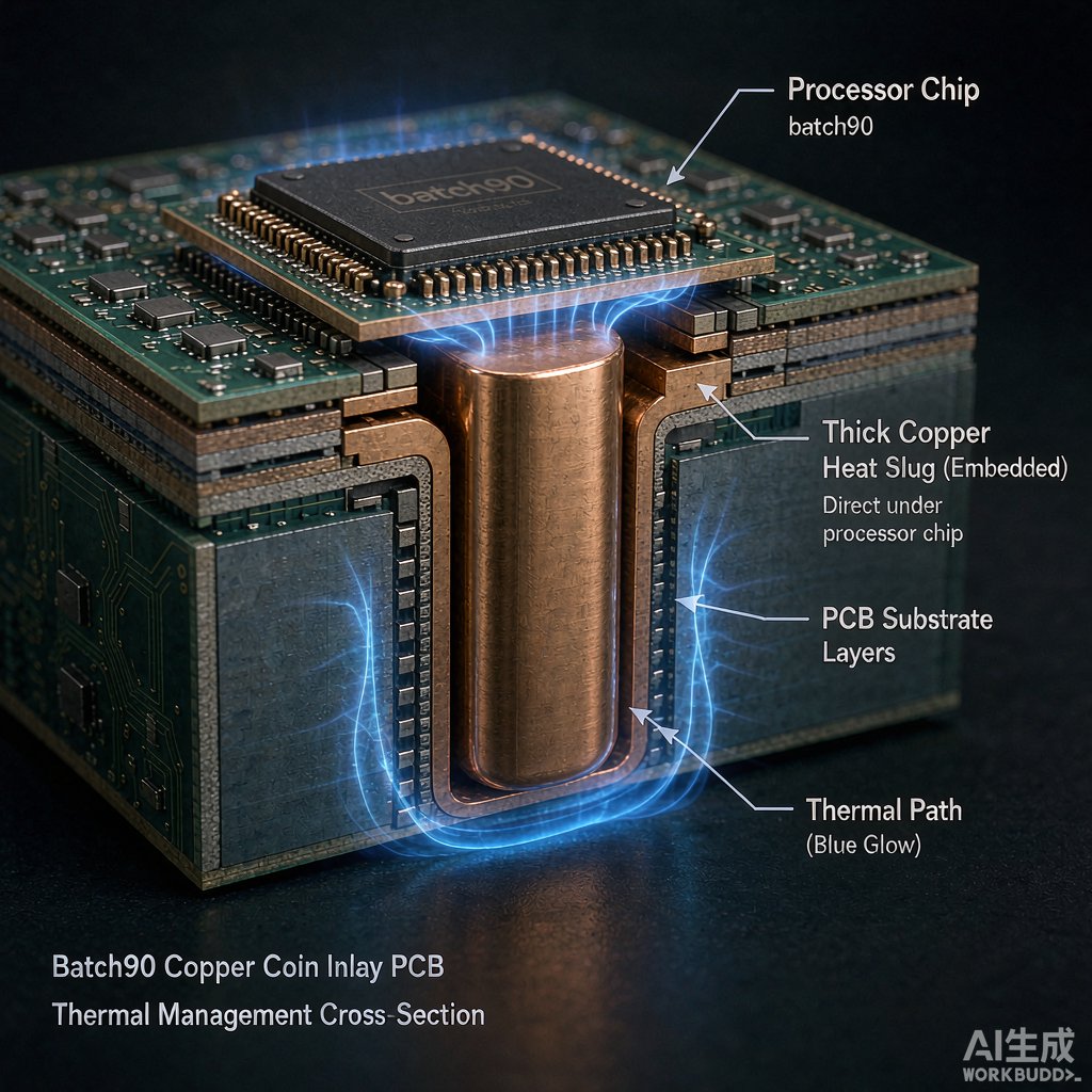
Modern SoCs, FPGAs, and RF power amplifiers concentrate tens of watts into a few square centimeters. Standard FR-4 spreads heat poorly — about 0.3 W/m·K through-plane — so a hot spot directly under a die can run 20–30 °C above the rest of the board. While metal-core PCB and thermal via fields help board-wide, a copper coin inlay PCB attacks the problem locally: a thick copper slug embedded under the heat source forms a dedicated thermal highway from the component to a heatsink or chassis. This technique is widely used in base stations, LED modules, and automotive power boards where PCB heat dissipation ca
ot be left to copper layers alone.
What Is a Copper Coin?
A copper coin is a solid copper piece — typically 1–3 mm thick — set into a milled pocket in the PCB, positioned directly beneath the heat-generating component. The coin may be electrically co
ected to a ground plane or isolated from all copper by the laminate. On the opposite side, the coin surface is exposed for direct contact with a heatsink or thermal interface material, creating a short, low-resistance path that bypasses several FR-4 layers entirely.
Three Mounting Variants
• Press-fit coins are mechanically pressed into a prepared opening before final lamination — the fastest and most economical variant.
• Soldered coins are reflowed with solder to improve thermal contact at the interface.
• Laminated (embedded) coins are bonded into the stack during pressing, giving the best planarity and thermal continuity.
Each variant trades cost, thermal resistance, and planarity, so the choice depends on assembly flatness tolerances and reliability targets.
How Much Cooling Do You Gain?
A typical 2 mm coin spa
ing 10 × 10 mm beneath a 15 W device lowers board-side thermal resistance dramatically compared with a via field. Supplier case studies report junction temperature reductions of 15–25 °C versus standard FR-4 construction with equivalent thermal vias, and 8–15 °C versus a metal-core PCB of the same footprint. The reason is simple geometry: the coin offers a solid copper cross-section hundreds of times larger than the combined barrel area of a via array.
Spreading Versus Removal
The coin does not remove heat by itself; it spreads it. Downstream, the heat still needs an exit — a heatsink clamped to the exposed coin face, a chassis mount, or airflow. Designers should size the coin at least 1.5–2 times the die footprint so the heat flux entering the copper is low enough for efficient spreading before it reaches the external interface.
Design Rules for Copper Coin PCBs
Successful coin integration depends on respecting a few mechanical and electrical boundaries:
• Keep signal routing at least 0.5 mm away from the coin edge to avoid dielectric thi
ing and impedance disruption
• If the coin is grounded, co
ect it to the ground plane through the surrounding plated ring; if isolated, maintain the creepage and clearance required by the working voltage
• Account for CTE mismatch: copper expands at about 17 ppm/°C against FR-4’s 14–16 ppm/°C, so large coins need stress-relief pockets or symmetric stack-up to prevent warpage after reflow
Stack-Up and Planarity
Coins add local thickness, and the surrounding laminate must compress evenly during pressing. Specify the pocket depth so the coin sits flush within ±0.05 mm of the board surface. Exposed coin faces on the heatsink side should be machined flat, and suppliers often offer coin-face milling or polishing to guarantee the flatness the TIM layer needs for predictable contact resistance.
Manufacturing Flow and DFM
Fabrication begins with milling the pocket in the i
er layers, inserting the coin, and laminating the stack. After lamination, the board is drilled and plated as usual, and the coin surface receives a finish such as ENIG, OSP, or bare copper with anti-tarnish treatment. Key DFM points: avoid placing vias within 0.3 mm of the coin edge, keep the coin away from panel edges to allow router handling, and check that the coin does not overlap high via-density zones near layer transitions. Lead time typically adds 3–7 days over standard PCB, and unit cost rises mainly with pocket milling time — small, simple coins keep the premium modest.
Inspection and Reliability Testing
Request cross-section samples to verify coin seating and laminate bond, plus thermal cycling — for example −40 to +125 °C for 500 cycles — to confirm no delamination around the coin. X-ray inspection checks for voids at the coin-to-laminate interface, which is the usual failure site when thermal performance drifts in the field.
When a Coin Beats the Alternatives
Choose a copper coin when one or two concentrated hot spots dominate the thermal budget, the rest of the board is conventional, and a heatsink can be mounted on the coin’s exposed face. For heat distributed across the whole board, an insulated metal substrate is more effective; for medium power and many small sources, thermal via arrays with thick outer copper usually suffice. For a single 10–30 W die on FR-4, however, the coin remains the most direct, proven, and comparatively affordable path to lower junction temperatures.