## Introduction
As wireless co
ectivity becomes standard in consumer, industrial, and automotive electronics, RF modules on the same PCB must coexist without mutual interference. Board-level electromagnetic interference (EMI) shielding cans — also known as shielding covers or Faraday cages — provide localized isolation for sensitive or noisy SMT circuits. They are cheaper than full enclosure-level shielding and can be placed directly over the offending circuit area after the main SMT assembly is complete.
This article presents practical design rules for selecting and implementing board-level EMI shielding cans on SMT RF modules, with a focus on aperture control, grounding integrity, and solder joint reliability.
## Shielding Can Construction
### Frame and Lid
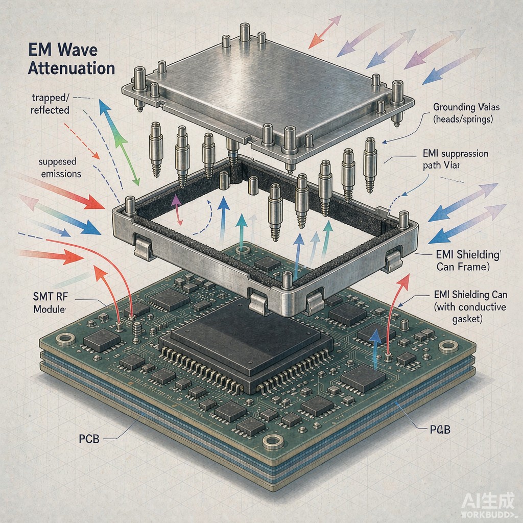
A typical board-level shield consists of a solder-down frame and a removable lid. The frame is a stamped metal perimeter with small feet or tabs that are reflow-soldered to the PCB. The lid snaps or slides onto the frame, allowing access for tuning, inspection, or rework without desoldering the entire shield.
Materials include tin-plated cold-rolled steel, nickel-silver alloy, brass, and stainless steel. Tin-plated steel is the most common choice because it solders well, provides adequate shielding above 1 GHz, and is inexpensive. For marine or outdoor applications, nickel-silver or stainless steel offers better corrosion resistance.
### Apertures and Shielding Effectiveness
No shield is perfectly sealed. Ventilation holes, seams between lid and frame, and cutouts for coaxial cables all leak electromagnetic energy. The shielding effectiveness at a given frequency depends on the largest linear aperture dimension, not the total open area. As a rule of thumb, the longest aperture edge should be smaller than one-twentieth of the wavelength of the highest frequency to be contained.
For a 5 GHz Wi-Fi module, the wavelength in air is 60 mm, so aperture dimensions should be below 3 mm. For 28 GHz mmWave systems, aperture dimensions must shrink to roughly 0.5 mm, often requiring conductive mesh or plated plastic covers rather than simple stamped holes.
## PCB Layout and Grounding Rules
### Ground Ring and Vias
The shield frame must co
ect to a continuous ground ring on the PCB. This ring should be at least 1.0 mm wide and located on all copper layers, stitched together with vias spaced 2–3 mm apart around the perimeter. The via fence reduces the impedance between the shield frame and the ground plane and prevents common-mode currents from circulating on the PCB surface.
Avoid routing high-speed traces or power planes under the shield ring unless they are tightly coupled to ground. A noisy trace located directly beneath the frame can couple energy into the shield structure and re-radiate it elsewhere.
### Solder Joint Design
Each foot of the shield frame forms an SMT solder joint. The foot width is typically 0.6–1.0 mm, and the recommended stencil aperture is slightly smaller than the foot pad to control solder volume. Too much solder causes the frame to float or tilt; too little solder creates a weak joint that may fracture under vibration or during lid removal.
For automated optical inspection, leave at least one visible corner foot unobstructed by components. This allows AOI systems to verify wetting and fillet quality after reflow.
## Multi-Cavity and Two-Piece Shields
When multiple RF circuits share the same module, a single large shield may permit cavity-to-cavity coupling. Multi-cavity shields use internal walls soldered to ground traces on the PCB, isolating transmitter, receiver, and local oscillator sections. The same aperture and grounding rules apply to the internal walls.
Two-piece shields with snap-on lids simplify rework but require adequate retention force. If the lid will be removed frequently during production tuning, specify a higher spring force or add small detents in the frame design.
### Assembly and Rework Process
Shield frames are typically placed by pick-and-place machines using the same solder paste stencil as other SMT components. Because frames are relatively large and lightweight, vacuum nozzles must be selected carefully to prevent deformation during placement. After reflow, frames are inspected for coplanarity; a twisted frame creates gaps that leak RF energy and may prevent the lid from seating properly.
Rework of shield frames is straightforward because they have exposed metal tabs. A hot air station with a large nozzle can reflow all feet simultaneously, allowing the frame to be lifted without disturbing nearby small components. For two-piece designs, only the lid is removed for tuning, and the frame remains soldered to the PCB.
### Shielding Effectiveness Measurement
After assembly, shielding effectiveness can be verified with near-field probes, spectrum analyzers, or transverse electromagnetic cell testing. A common production test is to compare the noise floor of the RF module with the lid on and off. A well-designed shield should reduce coupled noise by at least 20–40 dB across the operating bandwidth. If the improvement is less than expected, check for missing ground vias, excessive aperture size, or poor solder fillets at the frame feet.
## Conclusion
Board-level EMI shielding cans are an effective, low-cost way to isolate RF modules in dense SMT assemblies. Successful implementation depends on controlling aperture dimensions, maintaining a low-impedance ground co
ection around the entire perimeter, and designing robust solder joints that survive assembly, test, and field use.