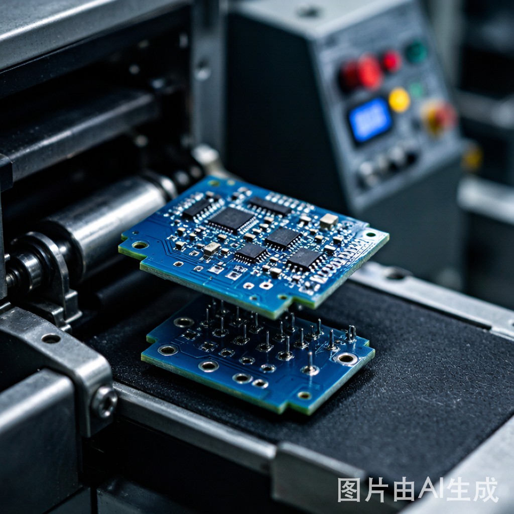
Most modern electronic assemblies use both sides of the PCB. A typical design might place fine-pitch BGAs and QFNs on the top side, with discretes, co
ectors, and occasionally larger ICs on the bottom side. The double-sided SMT assembly process is well established in high-volume production, but it introduces thermal management challenges that don’t exist in single-sided assembly. The most critical of these is reflow profiling — the same board will pass through the reflow oven twice, and the second pass must reflow the second-side solder joints without re-melting or damaging the first-side components.
Two Reflow Strategies
There are two fundamentally different approaches to double-sided SMT assembly, and the choice depends on the board’s component mix:
Sequential reflow with second-side adhesive (also called “pin-in-paste” or “double reflow with glue”): Both sides are populated with solder paste, but the bottom-side components (those that will be soldered second) are first glued to the board with a small dot of SMT adhesive. The first reflow solders the top-side components, and the adhesive holds the bottom-side components in place when the board is flipped and the second reflow is performed. This approach works well when the bottom-side components are relatively small and light (resistors, capacitors, small ICs).
Simultaneous reflow (no adhesive): Both sides are populated with solder paste, and the board passes through the reflow oven once, upside-down, with both sides reflowing simultaneously. The surface tension of the molten solder and the weight of the components must be sufficient to hold components in place during the thermal cycle. This works only when the bottom-side components are small, lightweight, and have a favorable pad geometry. Larger components (BGAs, QFNs, transformers) will fall off or shift if not glued.
The sequential approach with adhesive is the dominant method in production because it supports a wider range of component sizes and reduces defect rates. The simultaneous approach is reserved for very simple boards (LED strips, basic consumer electronics with only chip components on the bottom side).
First-Side Reflow Profile Considerations
The first-side reflow is typically the simpler of the two. The board starts as a bare PCB with components only on one side, so there is no risk of disturbing already-soldered joints. The first-side profile should be optimized for the most demanding component on the first side — typically the BGA or QFN with the tightest thermal budget.
Standard first-side reflow parameters for SAC305 lead-free solder paste:
- Preheat ramp: 1.0–2.0°C/s from ambient to 150°C
- Soak: 60–90 seconds at 150–200°C for flux activation and thermal equilibrium
- Ramp to peak: 1.0–1.5°C/s from 200°C to peak
- Peak temperature: 235–245°C at the thermocouple measuring the largest thermal mass component
- Time above liquidus (TAL): 45–75 seconds
- Cool-down: 2.0–3.0°C/s
The peak temperature and TAL are critical for BGA and QFN components with central thermal pads. The center of a BGA typically runs 5–10°C cooler than the edges during reflow (due to the thermal mass of the package and the PCB’s thermal mass under the part). Profile the oven with thermocouples at the BGA center AND at the BGA edge to ensure both meet the reflow requirements.
Second-Side Reflow: The Critical Pass
The second-side reflow is where most double-sided reflow defects originate. Three failure modes are unique to the second pass:
Failure mode 1: First-side components falling off. During the second reflow, the board is upside-down. The first-side components — which were soldered in the first pass and are now at the top of the oven — are held in place only by the surface tension of their solidified solder joints. If the joint temperature approaches the SAC305 solidus (217°C), the joint can soften and the component can shift or fall.
Mitigation: Keep the second-side peak temperature at the first-side joint location below 200°C — well below the SAC305 solidus. This is typically achieved by:
- Using a slightly lower peak temperature in the second pass (230–238°C vs 240–245°C in the first pass).
- Reducing the second-pass TAL by 10–15 seconds compared to the first pass.
- Using double-sided board thermocouple profiling to measure the first-side component temperature during the second pass and adjust the oven profile to keep it below 200°C.
Failure mode 2: Second-side component shift. If the second-side components are not glued (or are inadequately glued), they can shift when the solder melts during the second reflow. The combination of board vibration in the oven conveyor and the surface tension of the molten solder can drag components 0.1–1.0 mm from their design position, causing bridging or opens.
Mitigation: Use a high-quality SMT adhesive (e.g., Loctite 3609, Henkel QMI536) dispensed in a 1.0–2.0 mm diameter dot under each component body. Cure the adhesive during the first reflow (or in a separate UV/thermal cure step for UV-curable adhesives). For larger components (BGAs > 15 mm, QFNs > 10 mm), dispense two adhesive dots to provide redundant holding force.
Failure mode 3: Solder joint thermal degradation. Even if the first-side joint doesn’t melt, exposure to the second-side reflow’s thermal cycle ages the joint. The intermetallic layer at the copper-solder interface grows during each thermal excursion, and the Cu₆Sn₅ layer at the interface becomes thicker with each reflow cycle.
Mitigation: Limit total thermal exposure to 3 reflow cycles maximum (including rework). For double-sided assembly with possible rework, this means: 1 reflow for first side + 1 reflow for second side + 1 allowed rework cycle = 3 total. Beyond 3 cycles, the intermetallic layer becomes thick enough to embrittle the joint, particularly with ENIG surface finish where the Ni-Sn intermetallic adds an additional failure mode.
Adhesive Selection and Application
SMT adhesive selection depends on the components being glued, the reflow profile, and the board’s downstream processes:
| Adhesive Type | Cure Method | Application | Strength | Process Notes |
|---|---|---|---|---|
| Thermal cure epoxy (1-part) | Heat, 30 min @ 150°C or 5 min @ 180°C | General purpose | High | Adds separate cure step |
| Snap-cure epoxy (1-part) | Heat, 1–3 min @ 150°C | High-volume | High | Cures during preheat of reflow |
| UV-curable adhesive | UV light, 5–30 s | Selective cure, repairable | Medium | Requires UV access |
| UV + moisture dual cure | UV + ambient moisture | Shadowed areas + UV areas | High | Versatile |
| Pressure-sensitive (tape) | None (mechanical bond) | Prototype, low-volume | Low | Not for production |
The dominant choice for high-volume production is snap-cure epoxy that cures during the preheat phase of the first reflow, eliminating the need for a separate cure oven. The adhesive is dispensed before component placement, the components are placed on top of the adhesive dots, and the first reflow’s preheat cures the adhesive before the solder paste reaches reflow temperature.
Adhesive dot size and placement are critical:
- Dot diameter: 1.0–2.5 mm, depending on component size. Small chip components (0402, 0603) use 0.8–1.2 mm dots. Larger components (SOIC, QFP) use 1.5–2.5 mm dots.
- Dot location: Center of the component body, or under the heaviest portion (e.g., the die area of a BGA). Multiple dots for large components.
- Dot volume: Typically 0.05–0.5 mm³. Insufficient volume produces weak bonds; excessive volume causes the adhesive to spread into the solder pads and create defects.
Board Warpage Control
Double-sided SMT assembly amplifies board warpage. The first reflow heats the board asymmetrically (components on one side, copper on the other), creating thermal stress. The second reflow adds more. Asymmetrical copper distribution (heavy ground planes on one side, signal traces on the other) compounds the problem. Excessive warpage causes:
- Pick-and-place positioning errors: If the board warps more than 1.0 mm between support points, the placement machine’s vision system ca
ot accurately position components.
- Stencil printing gaps: A warped board does not make consistent contact with the stencil, causing printing defects.
- Reflow defects: A warped board in the oven does not lie flat on the conveyor, causing uneven heating and tombstoning.
Warpage mitigation for double-sided boards:
- Symmetrical copper: Distribute copper evenly across both sides of the board. If a heavy ground plane is needed on the top side, add a similar copper pattern (even dummy copper) on the bottom side. Modern design tools can automatically balance copper density.
- Use high-Tg laminate: Tg > 150°C (preferably 170°C) for lead-free double-sided assembly. Standard FR-4 (Tg 130–140°C) is borderline acceptable.
- Use thicker boards: 1.6 mm is the standard; thi
er boards (0.8–1.2 mm) warp much more easily.
- Support in oven: Heavy or large boards (> 250 × 350 mm) may need center support in the oven to prevent sagging.
- Pre-bake boards: For boards with high moisture sensitivity (MSL 3+), pre-bake at 125°C for 2–4 hours before assembly to drive off absorbed moisture and prevent blistering during reflow.
Process Validation
A new double-sided SMT process should be validated through a structured ramp:
- First-pass yield baseline: Build 50 boards, measure first-pass yield for each side separately. Target: 98%+ for both sides.
- Cross-section analysis: After both reflows, cross-section sample 5 boards to verify joint integrity, intermetallic thickness, and absence of voids.
- Thermal cycling reliability: Run 100 boards through -40°C to +125°C thermal cycling for 1,000 cycles. Verify no first-side joint failures and no delamination.
- Adhesive strength testing: Apply a shear force to glued components and verify the adhesive can withstand > 5× the component weight without releasing.
- SPI and AOI coverage: Verify 100% SPI coverage on both sides and 100% AOI coverage after each reflow. Capturing defects between the first and second reflows prevents propagation.
For high-volume Southeast Asian SMT production — consumer electronics, industrial controls, automotive ECUs — double-sided reflow is a standard capability, but the process control discipline is significantly higher than single-sided assembly. The cost of a single first-side component falling off during the second reflow — board scrap, component scrap, and the time to diagnose and reset the line — typically exceeds $5 per occurrence. Multiply by thousands of boards per month, and a 0.1% defect rate from inadequate process control adds $50,000+ per year in avoidable cost. The discipline is to treat the double-sided reflow process as a tightly controlled manufacturing operation with measurement at every step, not as a “just run it twice” afterthought.