For most SMT assembly, solder paste applied through a stencil is the obvious choice. The paste deposits the precise volume needed for each pad, the process is fast and repeatable, and the equipment is widely available. But there are assembly scenarios where solder paste is the wrong tool — applications requiring larger solder volumes, void-free joints under high thermal stress, or precision solder placement independent of a stencil. In these cases, solder preforms — pre-cut pieces of solder alloy in defined shapes and sizes — offer advantages that paste ca
ot match.
What is a Solder Preform?
A solder preform is a precisely manufactured piece of solder alloy, cut or stamped to a specific shape and size, with a tightly controlled mass. Common formats include:
- Discs: Round washers of solder, typically 0.5–10 mm diameter and 0.05–0.5 mm thick. Used in thermal interface applications, RF co
ector shields, and through-hole pin soldering.
- Rectangles and squares: For surface-mount power components, large QFN thermal pads, and baseplate soldering.
- Rings and frames: For sealing applications, ceramic package soldering, and large-area hermetic seals.
- Wire and ribbon: For hand-soldering and specialized automated placement.
Preforms are manufactured by stamping, etching, or progressive die cutting of rolled solder sheet. The typical mass tolerance is ±2–5%, far tighter than the 10–20% volume variation commonly seen in stencil-printed solder paste.
Volume Control and Joint Consistency
Stencil-printed solder paste has unavoidable volume variation. Even with a high-quality stencil and well-controlled process, the coefficient of variation (CoV) of paste deposit volume is typically 10–15%. After reflow, this variation translates directly to variation in joint standoff height and fillet geometry.
For components sensitive to standoff height — power QFNs, BTCs (bottom-terminated components), LEDs requiring precise optical centering, and large BGAs with thermal pad co
ections — paste volume variation can produce:
- Excessive standoff: Too much paste produces a tall joint, increasing thermal resistance and reducing mechanical robustness.
- Insufficient standoff: Too little paste produces a thin joint that may not meet IPC-A-610 minimum fillet requirements.
- Tombstoning and skewing: Unequal paste volume on opposite ends of a passive component creates differential wetting forces that lift one end of the part.
Preforms, by contrast, have a defined mass and geometry. When placed consistently and reflowed under controlled conditions, the resulting joint volume and standoff height are remarkably repeatable. For thermal pad applications, standoff heights can be controlled to ±10 μm, compared to ±50 μm typical for paste.
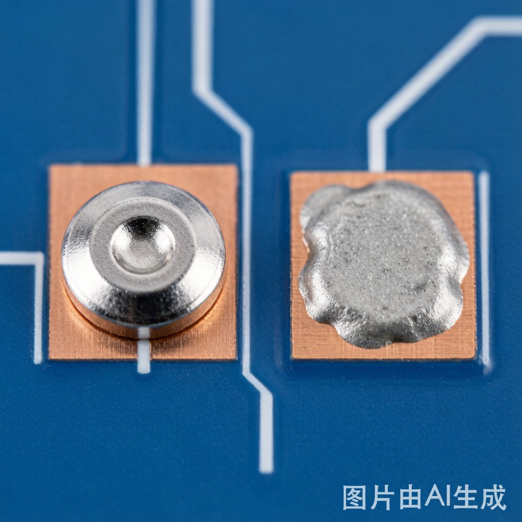
Void Reduction in Power Electronics
The single biggest application advantage of solder preforms in power electronics is void reduction in large thermal pad joints. A power QFN with a 6×6 mm thermal pad, when soldered with paste, will typically exhibit 15–30% voiding in the joint — voids are the gas bubbles trapped in the solder as flux outgasses during reflow. These voids dramatically increase thermal resistance:
| Void Content | Thermal Resistance Increase | Junction Temp Rise (10W dissipation) |
|---|---|---|
| 5% (excellent paste) | +5% | +1.5°C |
| 15% (typical paste) | +15% | +4.5°C |
| 30% (poor paste) | +35% | +10.5°C |
| 50% (worst case) | +60% | +18°C |
A preform placed on the thermal pad before component placement provides a uniform, dense solder volume with minimal flux to outgas. The result: void content typically 1–3%, with the best processes achieving <1% voiding.
Preform-based void reduction is widely used in:
- Power MOSFET and IGBT modules: D²PAK, TO-220, and direct-bonded copper (DBC) substrate soldering.
- High-brightness LED packages: LED thermal pad soldering where 1% void reduction can extend LED lifetime by 5–10%.
- RF power amplifier modules: GaN and LDMOS transistors where thermal resistance directly limits output power.
- Automotive power modules: AEC-Q100 qualified assemblies with strict thermal management requirements.
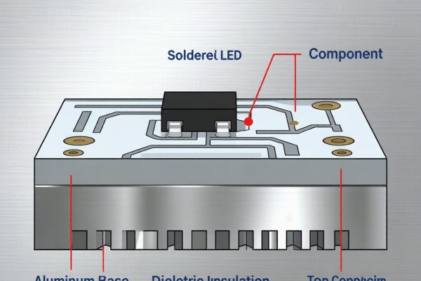
Thermal Interface Performance
For power modules and LED assemblies, the solder joint itself is part of the thermal path from the die to the heatsink. A preform-soldered joint has several thermal advantages over a paste-soldered joint:
- Lower thermal resistance: The dense, low-void preform joint has 0.5–1.5°C/W lower thermal resistance per cm² than a typical paste joint, due to higher thermal conductivity (50–60 W/m·K for dense SnPb or SAC vs 25–40 W/m·K for paste-derived joints with voids).
- Predictable standoff: Preform thickness sets the standoff height precisely. For a 0.1 mm thick preform, the post-reflow standoff is 0.08–0.10 mm, depending on wetting. This predictable spacing is critical for thermal interface material (TIM) selection downstream.
- Better mechanical compliance: A slightly thicker standoff from a preform provides compliance that absorbs thermal expansion mismatch between the die and the substrate, reducing stress on the die and the surrounding interco
ects.
Placement Methods for Preforms
Preform placement uses three principal methods, each suited to different production scales:
Manual placement: Operators pick and place preforms using tweezers or vacuum pens. Suitable for prototype and low-volume work (1–100 pieces per day). Preform orientation is critical — even small misalignment causes uneven joint formation.
Pick-and-place with custom tooling: Standard SMT pick-and-place machines can be fitted with preform-specific nozzles that pick from a waffle tray, matrix tray, or tape-and-reel format. Vision systems verify preform position before placement. Suitable for medium-volume production (100–10,000 pieces per day).
Dedicated preform placement machines: Specialized equipment (e.g., Indium Corp, EFD, or Heller preform placers) that combine flux dipping, preform placement, and component placement in a single station. Highest throughput and best process control, but capital investment $150,000–$400,000.
Reflow Profile Considerations
Solder preforms require a slightly different reflow profile than solder paste, primarily because of the absence of flux solvents and the lower surface-area-to-volume ratio:
- Preheat: 90–120 seconds ramp from 50°C to 150°C. Slower than paste preheat to allow the preform to reach thermal equilibrium with the board.
- Soak: 60–90 seconds at 150–180°C. Flux activation temperature; the preform has not yet started to melt but the flux must be fully active before the solder wets.
- Time above liquidus (TAL): 45–75 seconds for SAC305, 30–60 seconds for SnPb. Slightly longer than paste reflow to ensure the preform fully melts and wets the pad and lead.
- Peak temperature: 235–245°C for SAC305, 215–225°C for SnPb. Same as paste reflow.
- Cool-down: ≤3°C/s to avoid shocking the joint and creating intermetallic cracks.
For void-sensitive applications, vacuum reflow soldering is the gold standard. A vacuum reflow oven pulls 50–100 mbar absolute pressure during the TAL phase, evacuating dissolved gases in the molten solder. Combined with preforms, this technique can achieve <0.5% void content, satisfying the most demanding automotive and aerospace requirements.
Cost Analysis
Solder preforms cost more per unit mass than solder paste, reflecting the additional manufacturing steps (stamping, mass verification, packaging):
| Format | Alloy | 2026 Southeast Asia Price (USD/kg) | Premium vs Paste |
|---|---|---|---|
| SAC305 solder paste (Type 3, no-clean) | SAC305 | $65–85 | 1.0× (baseline) |
| SAC305 preform (stamped disc) | SAC305 | $110–140 | 1.6× |
| SAC305 preform (etched frame) | SAC305 | $140–180 | 2.0× |
| SnPb preform (mil-spec) | Sn63/Pb37 | $90–120 | 1.3× |
| AuSn preform (high-reliability) | Au80/Sn20 | $3,500–4,500 | 50× (gold content) |
For a power QFN with a 6×6 mm thermal pad, the preform mass is approximately 0.10 g. At $125/kg, the per-piece preform cost is $0.0125. The cost premium over paste (~$0.008) is $0.0045 per joint. For an automotive power module with 8 such joints, the total preform cost premium is $0.036 per module. This is trivial against the value of a 5% void reduction that may extend module warranty coverage by 12–24 months.
Application Selection Guide
Choose solder paste when:
- Standard SMT assembly (resistors, capacitors, ICs) with no special thermal or void requirements
- High-volume production where throughput is the dominant driver
- Component standoff height is not critical to downstream processes
- Cost per joint must be minimized
Choose solder preform when:
- Large thermal pad co
ections where voiding must be <5%
- LED assembly where joint standoff and void content directly affect optical performance
- High-reliability applications (automotive, aerospace, medical) where joint consistency is non-negotiable
- Hermetic sealing or solder die-attach where precise solder volume is required
- Hand-soldering or selective placement where stencil printing is impractical
For the broader SMT market, paste remains the default — preforms occupy a specialized but growing niche driven by the power electronics and high-brightness LED industries. The trend is favorable: as power densities increase and thermal management becomes more critical, the use of preforms is expanding into applications where paste-based assembly previously dominated.