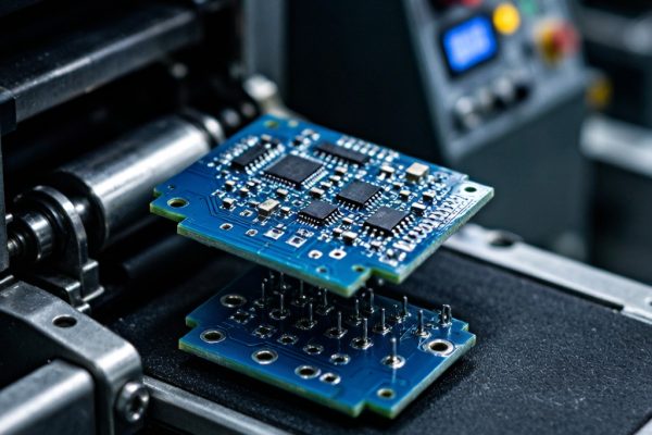
When a board carries both surface-mount components on the top side and through-hole parts on the bottom, the classic dilemma is: how do you solder the through-hole leads without re-melting or washing off the SMT solder joints already on the board? The traditional answer — full-board wave soldering — works only when SMT components are spaced well away from the wave. As component density has climbed, that condition has become rare. Selective wave soldering is the modern solution: a small, programmable solder nozzle that dispenses a localized wave of molten solder onto individual through-hole joints or clusters of joints, while leaving the surrounding SMT components untouched.
How Selective Wave Soldering Differs from Full Wave
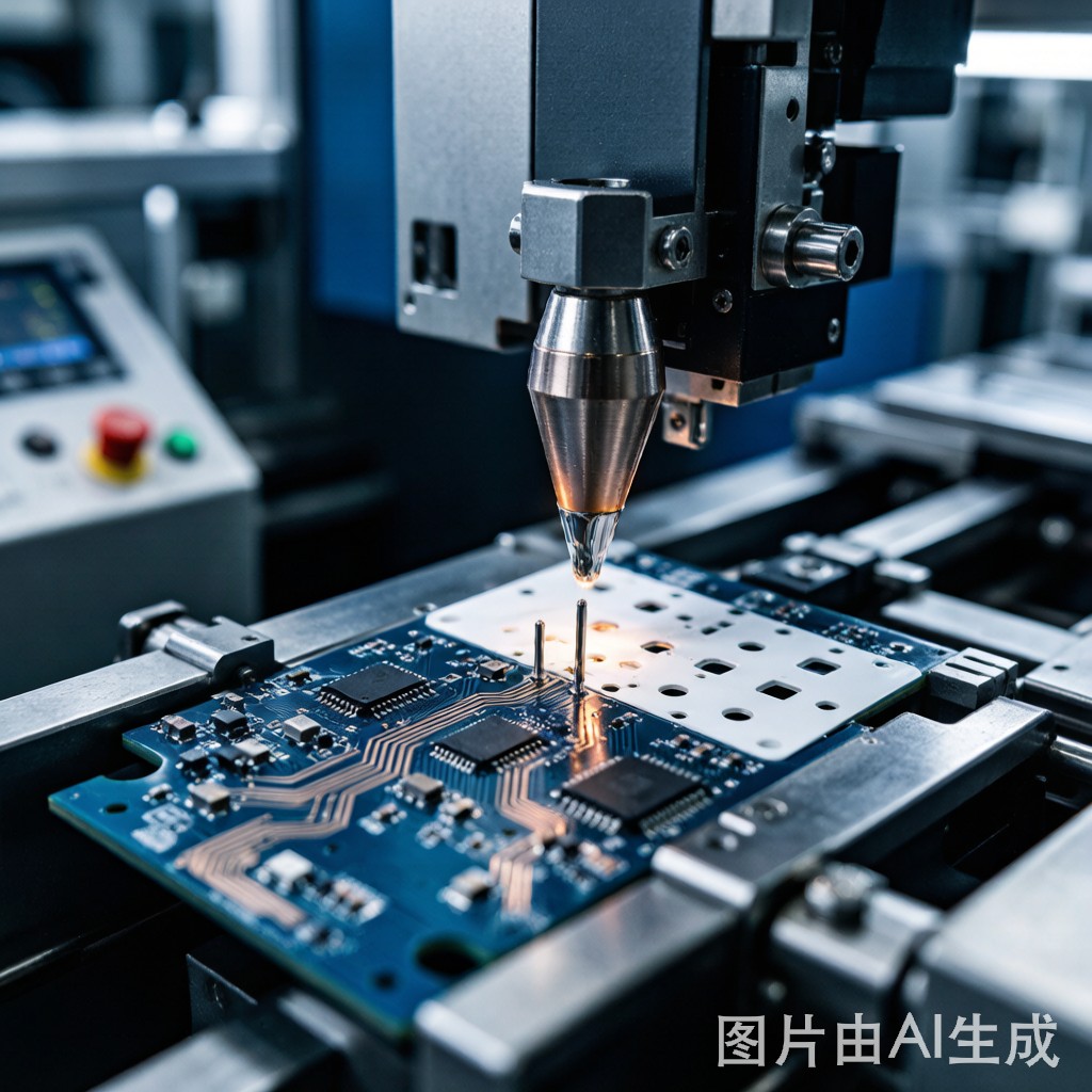
A full wave soldering machine floods the entire bottom of the board with a wide, dynamic wave of solder. Selective soldering, by contrast, uses a small nozzle (typically 5–30 mm in diameter) that pumps solder upward through an opening aligned with a single pin or small group of pins. The board is held above the nozzle on an X-Y-Z programmable stage, and each through-hole joint is soldered in sequence by moving the board into position over the nozzle for a controlled dwell time.
The key advantages of selective soldering versus full wave are dramatic:
- No solder mask on SMT pads: SMT components on the bottom side of the board (BGAs, QFNs, chip resistors) remain untouched, eliminating the need for solder resist dams, peelable solder masks, or fixture-based solder masking that full-wave mixed-assembly requires.
- Lower thermal stress: Only the localized through-hole area is exposed to 260°C+ solder. SMT components see only the board’s preheat temperature (typically 100–150°C), well below their reflow rating.
- No solder bridging on fine-pitch SMT: Full wave creates turbulence that can splash solder onto fine-pitch pads and create shorts. Selective soldering is essentially static during the dwell, so fine-pitch parts are not at risk.
- Process flexibility: The X-Y stage can be programmed to skip specific joints, change dwell time per joint, and apply different flux volumes to different joint types.
Selective Soldering Nozzle Types
Three nozzle designs dominate production. The choice depends on the through-hole geometry, board layout, and volume.
| Nozzle Type | Typical Diameter | Best Application | Wetting Time |
|---|---|---|---|
| Mini-wave | 5–10 mm | Single pins, small co
ectors, fine-pitch headers |
1.0–2.0 s |
| Jet-wave | 10–20 mm | Row of pins, D-sub co
ectors, pin headers |
1.5–3.0 s |
| Dip-wave | 20–30 mm | Large co
ectors, multiple adjacent joints, power components |
2.0–4.0 s |
Mini-wave nozzles produce a tall, narrow solder column (4–6 mm above the nozzle rim) that pins the through-hole lead and barrel in a fountain of solder. These are ideal for single pins, where the surrounding SMT components are within 1–2 mm of the through-hole pad and the board ca
ot tolerate excess solder spread. Mini-wave typically uses a non-wettable nozzle material (titanium or stainless steel) with a precisely machined wettable tip insert that defines the wave geometry.
Jet-wave nozzles use a higher-velocity solder stream that penetrates the through-hole barrel and wets the lead on both top and bottom. The jet flow also helps evacuate flux gases from the hole, reducing blowholes and voids in the joint. Jet-wave is the workhorse for co
ector rows and D-sub pins where multiple joints are soldered in a single pass.
Dip-wave nozzles produce a wide, low-profile wave that contacts the entire component lead group simultaneously. Used for large co
ectors, power transistor leads, and through-hole transformers where uniformity across multiple joints is critical.
Flux Deposition and Preheat
Selective soldering uses two flux application methods: drop-jet fluxing (most common) and micro-spray fluxing. Drop-jet fluxers dispense a precise droplet (0.5–5.0 μL) of flux onto each through-hole pad, with programmable volume per joint. Micro-spray fluxers atomize flux into a fine mist that deposits on a defined area. Drop-jet is preferred for high-reliability and high-volume production because flux volume is precisely controlled and overspray is minimized.
Preheat is critical. In a typical selective soldering line, the board passes through a preheat zone that raises the bottom-side temperature to 100–140°C before reaching the solder nozzle. Preheat serves three functions: drives off flux solvents, activates the flux chemistry, and reduces thermal shock at the solder nozzle. Insufficient preheat is the most common cause of selective soldering defects — particularly blowholes and poor hole fill — because the board’s thermal mass cools the solder on contact, shortening the wetting window.
For lead-free selective soldering with SAC305 or SnCu alloys, target preheat values are:
- Bottom-side preheat temperature: 120–150°C measured at the board surface, immediately before the solder nozzle.
- Preheat time: 60–180 seconds depending on board mass and copper coverage. Heavy copper boards (3+ oz) may need 200+ seconds to reach equilibrium.
- Preheat delta-T (top to bottom): < 20°C for double-sided assemblies. Large deltas can cause SMT components on the top side to reflow prematurely.
Nozzle Immersion Depth and Dwell Time
The two process parameters that most directly affect joint quality are nozzle immersion depth (how far the board is lowered into the wave) and dwell time (how long the board remains in contact with the wave). Recommended starting values for lead-free SAC305:
| Parameter | Mini-Wave | Jet-Wave | Dip-Wave |
|---|---|---|---|
| Nozzle temperature | 300–320°C | 290–310°C | 285–305°C |
| Immersion depth | 1.0–2.5 mm below pad top | 0.5–2.0 mm | 0.5–1.5 mm |
| Dwell time | 1.0–2.5 s | 1.5–3.5 s | 2.0–4.5 s |
| Pull-up ramp rate | 1.0–2.0 mm/s | 1.5–3.0 mm/s | 2.0–4.0 mm/s |
Immersion depth must be set so the wave covers the entire through-hole barrel plus a small margin above the top pad surface (typically 0.5–1.0 mm above). Insufficient depth leaves the top of the joint cold, producing an incomplete fillet. Excessive depth causes solder to climb the lead and create an icicle.
Dwell time must be long enough for the through-hole barrel to reach thermal equilibrium and for capillary action to wick solder up the barrel. Insufficient dwell is the most common cause of “blowhole” defects — gas trapped in the barrel escaping during solidification, leaving a void in the joint. Excessive dwell can dissolve copper from the pad (typical 1.0–1.5 μm per second of contact at 300°C) and weaken the joint.
Nitrogen Atmosphere Benefits
Selective soldering machines can be specified with an N₂-atmosphere enclosure surrounding the solder pot and preheat area. Holding the local atmosphere at <500 ppm O₂ reduces dross formation on the solder pot by 80% or more, and improves wetting on difficult surfaces (aged chem-tin, OSP-coated pads, nickel-plated through-holes).
For mixed-technology boards with bottom-side SMT components that are sensitive to solder flux splatter, N₂ atmosphere also reduces the rate of solder ball formation on adjacent SMT pads. The capital cost premium of 25–40% versus air atmosphere is typically recovered within 18–30 months through reduced dross disposal, lower solder consumption, and improved first-pass yield.
Defect Modes and Process Adjustments
The four most common selective soldering defects, and the corresponding adjustments:
Blowholes (voids in joint): Preheat too low, dwell time too short, or contaminated through-hole barrel. Increase preheat by 10–15°C, extend dwell by 0.5–1.0 s, and verify hole cleanliness.
Insufficient hole fill (less than 75% of barrel filled with solder): Insufficient immersion depth, low pot temperature, or fast pull-up rate. Increase immersion by 0.3–0.5 mm, raise pot temperature by 5°C, and reduce pull-up rate to allow solder to wick up before solidifying.
Icicles on joint bottom: Excessive immersion depth, low preheat, or slow pull-up. Reduce immersion by 0.3–0.5 mm and increase pull-up rate to create a clean peel-off.
Solder bridges between adjacent pins: Wave height too high, flux solids too low, or pads too close. Reduce wave height by 0.5–1.0 mm, increase flux solids content, or check that pad spacing meets the 1.0 mm minimum recommended for selective soldering.
Process Validation and Quality Control
A new selective soldering program should be validated through a 4-stage ramp:
- First article: Single board, all joints inspected via cross-sectioning. Verify hole fill, intermetallic formation, and joint geometry against IPC-A-610 Class 2 or Class 3 as specified.
- 50-board pilot run: Visual inspection of every joint on every board. Measure first-pass yield. Target: 99%+ for Class 2, 99.5%+ for Class 3.
- DOE optimization: 25-board design of experiments varying pot temperature, preheat, dwell, and flux volume. Use response surface methodology to identify the optimal process window.
- Production control: Statistical process control on key parameters (pot temperature, flux specific gravity, first-pass yield). Out-of-control conditions trigger line stop and process reset.
For Southeast Asian contract manufacturers producing industrial controllers, automotive ECUs, and power electronics, selective wave soldering has become the standard for mixed-technology assembly. The capital investment of $200,000–$500,000 for a mid-range selective soldering system is recovered through higher yield, less rework, and the ability to quote on complex mixed-technology boards that would otherwise require expensive fixtures or hand-soldering operations.