While surface mount technology has captured the majority of new PCB assembly volume, wave soldering remains indispensable for through-hole components — co
ectors, transformers, electrolytic capacitors, power transistors, and large electromechanical parts — and for mixed-technology boards that combine SMT on the top side with through-hole on the bottom. In Southeast Asian contract manufacturing, wave soldering lines process millions of boards a
ually for industrial controllers, automotive ECUs, audio equipment, and power supplies.
The dominant wave soldering defects — solder bridges, solder webs, and icicles — share root causes in flux activation, preheat uniformity, and solder wave dynamics. Understanding the defect mechanisms is the foundation for effective process control.
Wave Soldering Process Overview
A modern lead-free wave soldering line consists of four sequential zones:
- Flux application zone: Foam fluxer, spray fluxer, or drop-jet fluxer deposits a thin film of liquid flux on the bottom-side pads and leads. Typical flux volume: 1.5–4.0 g per 100 cm² board area.
- Preheat zone: Bottom-side IR or convection heating raises the board to 100–140°C to activate the flux, drive off solvents, and reduce thermal shock at the solder wave. Preheat time: 60–180 seconds depending on board mass.
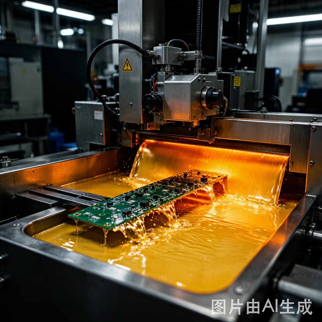
- Solder wave zone: Board contacts a flowing wave of molten SnCu or SAC alloy at 250–265°C. Contact time: 2–5 seconds. The dual-wave configuration (chip wave followed by main laminar wave) is now standard for mixed-technology boards.
- Cooling zone: Controlled cooling to 80–100°C before the board exits the machine, allowing solder joints to solidify with controlled grain structure.
Solder Bridges: The Most Common Defect
A solder bridge is an unintended solder co
ection between two adjacent conductors that should be electrically isolated. Bridges are the most common wave soldering defect, typically accounting for 30–50% of all defects at a wave soldering line.
Root cause 1: Excessive flux activity depletion. If the preheat temperature is too high (>150°C) or preheat time is too long (>180 seconds), the flux activity can be consumed before the board reaches the solder wave. The board then enters the wave with insufficient flux to break the surface tension of molten solder between adjacent pads, leading to bridging.
Root cause 2: Inadequate pad-to-hole ratio. The optimal pad diameter for through-hole wave soldering is 1.5–2.0× the finished hole diameter. Pads that are too small provide insufficient copper area to wick solder away from the gap between adjacent pads. Pads that are too close together (<0.5 mm spacing) provide insufficient clearance for clean solder separation.
Root cause 3: Excessive solder wave height. Wave height above the board surface should be 3–6 mm for the main wave. Excess wave height (8 mm+) causes solder to spill over the top side of the board and bridge components on the upper surface.
Root cause 4: Insufficient conveyor angle. Standard conveyor angle is 5–7° from horizontal. The angle creates a “peel-back” effect as the board exits the wave, helping to remove excess solder. Conveyor angles <4° result in poor peel-back and higher bridge rates.
Solder Webs and Solder Ball Defects
A solder web is a thin film of solder spa
ing a gap between two conductors, similar to a bridge but typically formed during the peel-back phase. A solder ball is a discrete sphere of solder that has detached from the main joint and adhered to the board surface, often near a non-wetted pad.
Web formation is primarily caused by:
- Slow peel-back rate: Conveyor speed below 0.8 m/min causes the solder to remain in contact with the pad for too long, allowing capillary action to span adjacent pads.
- Low solder pot temperature: Pot temperature below 250°C in lead-free wave soldering increases solder viscosity, reducing its ability to cleanly separate. Recommended: 255–265°C for SAC305 or Sn100C alloys.
- Contaminated solder pot: Copper dissolution into the solder pot raises the liquidus temperature and increases viscosity. Copper content should be maintained at 0.3–0.7% for SAC305 and 0.4–0.8% for SnCu alloys. Above 1.0% copper, drossing increases dramatically and bridge rates climb.
Solder ball formation is most often associated with:
- Excessive flux solids content: Fluxes with >25% solids content leave residual solids that can trap solder particles during cool-down, forming balls. Standard SMT-grade fluxes (15–20% solids) are acceptable for wave soldering, but fluxes designed specifically for wave (10–15% solids) produce fewer solder balls.
- Moisture in the laminate: PCBs that have absorbed moisture during storage release steam at the solder wave, splattering solder. Pre-baking at 105°C for 2–4 hours eliminates this.
- Poor solder mask adhesion: Solder mask lifting or peeling at the wave exposes laminate surface that is not protected by the hydrophobic mask, leading to solder ball retention. Verify solder mask adhesion per IPC-SM-840.
Icicles and Insufficient Solder Joints
An icicle is a downward-hanging point of solder protruding from a through-hole joint, caused by solder that did not fully wick up the through-hole barrel before solidifying. The opposite defect — insufficient solder — leaves the hole partially or completely unfilled, often exposing the lead tip.
Icicle formation is driven by:
- Board preheat too low: Preheat below 100°C fails to activate the flux and bring the board to thermal equilibrium. The thermal gradient from board to pad to lead causes the lead to be cooler than the pad, leading to premature solidification at the lead tip and icicle formation on the bottom side of the board.
- Excessive conveyor speed: Speeds above 2.0 m/min reduce contact time with the wave below 2 seconds, insufficient for solder to fully wet the through-hole barrel. Recommended: 1.0–1.5 m/min for lead-free wave soldering of mixed-technology boards.
- Lead-to-hole clearance too tight: The optimal clearance between lead and hole is 0.15–0.40 mm. Tighter clearances (capillary action too strong) cause solder to wick up the lead before fully filling the barrel. Excessive clearance (>0.5 mm) reduces capillary action and can leave voids or insufficient fill.
Insufficient solder joints result from:
- Holes with thermal barriers: Internal power/ground planes adjacent to a through-hole act as heat sinks, drawing heat away from the barrel and preventing full solder wetting. Solutions include “thermal relief” pad patterns (4 spokes co
ecting the pad to the plane) or longer contact time with the wave.
- Oxidized leads or pads: Component leads stored in uncontrolled environments develop oxide layers that resist wetting. Pre-ti
ed leads (Sn or SnPb coated) maintain solderability for 12+ months when stored properly. Uncoated copper leads should be soldered within 4–8 weeks of manufacture.
Process Window Optimization
Effective wave soldering process control requires monitoring the following parameters in real time and adjusting based on defect feedback:
| Parameter | Target Range | Adjustment Direction |
|---|---|---|
| Flux specific gravity | 0.810–0.830 (no-clean) | Higher = more solids = more residue |
| Preheat top board temp | 100–140°C | Higher = more flux activation, less thermal shock |
| Solder pot temperature | 255–265°C (SAC) | Higher = better wetting, more drossing |
| Wave height (above board) | 3–6 mm | Lower = less bridging, more icicles |
| Conveyor speed | 1.0–1.5 m/min | Faster = less contact, more icicles |
| Conveyor angle | 5–7° | Steeper = better peel-back |
| Copper in solder pot | 0.3–0.8% | Higher = more viscous, more bridges |
| Contact time with wave | 2.0–3.5 seconds | Longer = better hole fill, more thermal stress |
Nitrogen Atmosphere Benefits
While conventional wave soldering operates in air, nitrogen atmosphere wave soldering (O₂ < 1,000 ppm) has become increasingly common in Southeast Asian high-reliability assembly. The benefits include:
- Reduced dross generation: Dross (Cu₆Sn₅ and Cu₃Sn intermetallic oxides) forms on the solder pot surface from copper dissolution and oxidation. N₂ atmosphere reduces dross formation by 60–80%, decreasing solder consumption and pot maintenance frequency.
- Improved wetting on difficult surfaces: OSP-coated boards, aged lead-free pads, and nickel-plated through-holes all wet more reliably in N₂ atmosphere. This is particularly important for mixed-technology boards where SMT pads (various finishes) and through-hole pads (typically HASL or chem-tin) must be soldered simultaneously.
- Lower process temperatures possible: In N₂ atmosphere, the pot can be operated 5–10°C lower than in air while maintaining equivalent wetting performance. This reduces thermal stress on components and PCBs.
The capital cost of N₂ wave soldering systems is 30–50% higher than air-atmosphere systems, but for contract manufacturers ru
ing high-reliability product (automotive, industrial, medical), the defect reduction and lower solder consumption offset the capital premium within 18–36 months.
Post-Wave Inspection Strategy
Effective wave soldering quality control requires both automated and manual inspection steps:
- Inline AOI after wave: Bottom-side AOI systems detect bridges, webs, and missing/insufficient solder joints in real time. Typical false-call rate 2–5%; escaped defect rate <50 ppm for well-tuned systems.
- X-ray for BGA and bottom-terminated components: Mixed-technology boards often include BGA or QFN parts on the bottom side that are not visible to AOI. Transmission X-ray or 3D X-ray (CT) verifies solder joint integrity.
- Cross-section sampling: Destructive cross-sectioning of representative boards per lot verifies through-hole barrel fill, intermetallic formation, and laminate integrity. Sample rate 1–3 boards per 1,000 produced, or per IPC-9191 statistical process control guidelines.
For high-volume wave soldering operations in Southeast Asia, the cost of a single solder bridge that escapes to the field — a customer return, repair, and warranty expense — can exceed 100× the cost of ru
ing the wave soldering line with optimal process control. The discipline is to treat the wave soldering process as a tightly controlled manufacturing operation with measurable inputs, outputs, and feedback loops, not as a black-box step that “either works or doesn’t”.