In-circuit test (ICT) has been the workhorse of PCB electrical verification for over four decades. The principle is straightforward: a bed-of-nails fixture makes contact with designated test points on the powered-off board, applying a programmed sequence of analog and digital measurements to verify that every component is present, correctly oriented, and within specification. For high-volume SMT production in the hundreds of thousands of boards per year, ICT remains the most cost-effective way to catch manufacturing defects — short circuits, opens, wrong components, and out-of-tolerance values — before the board reaches functional test.
Designing an ICT fixture that delivers high fault coverage without false calls requires careful attention to test point accessibility, fixture mechanical design, and integration with the SMT assembly line.
The Bed-of-Nails Fixture: Mechanical Design
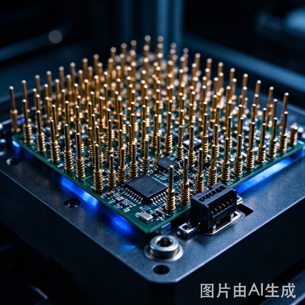
An ICT fixture is essentially a precision mechanical platform that holds the PCB in a defined position and brings hundreds or thousands of spring-loaded test probes (pogo pins) into contact with test points on the board. The main mechanical elements are:
- Top plate (probe plate): A drilled phenolic or aluminum plate that positions the upper pogo pins. The plate is drilled using NC machinery to ±0.05 mm positional accuracy relative to the PCB test point coordinates.
- Bottom plate (receiver plate): Holds the lower pogo pins and supports the PCB. May include vacuum cha
els to hold the board flat during testing.
- Pogo pins: Spring-loaded contact probes with a tip that contacts the test pad. Typical pogo pin specifications include:
- Tip style: Crown, pointed, chisel, or flat — selected based on test pad geometry
- Spring force: 100–300 grams (light force for fine-pitch, heavy for contaminated surfaces)
- Travel: 1.0–2.5 mm working stroke
- Rated life: 100,000 to 1,000,000 cycles
- Mechanical press: Pneumatic or servo press that brings top and bottom plates together with controlled force. Typical closure force 50–200 kg depending on pin count.
Test Point Design Rules
The quality of ICT fault coverage is fundamentally limited by test point accessibility. A test point that ca
ot be reliably contacted by a pogo pin is a test point that ca
ot be tested. The IPC-2221 and IPC-9191 standards provide detailed recommendations:
| Parameter | Minimum | Recommended | Notes |
|---|---|---|---|
| Test pad diameter | 0.8 mm | 1.0–1.5 mm | Smaller pads require pointed-tip pogo pins with reduced contact reliability |
| Pitch between test points | 1.27 mm (0.05 in) | 1.5–2.54 mm | Finer pitches require smaller-diameter pogo pins, more expensive fixtures |
| Distance from component body | 0.5 mm | 1.0 mm | Probe access for crown-tip pins |
| Distance from board edge | 3.0 mm | 5.0 mm | Edge proximity causes fixture plate interference |
| Test pad surface finish | HASL, ENIG, chem-tin | ENIG or chem-tin | OSP degrades contact reliability; HASL irregularity causes false opens |
| Test pad on component lead | 0.5 mm extension | Dedicated via or pad | Test point should be on a trace extension, not on the component lead itself |
For modern SMT boards with high component density, achieving 100% test point coverage often conflicts with signal integrity and routing density. The practical target is 85–95% test point coverage, with the remaining nets verified by flying probe, boundary scan (JTAG), or functional test.
Pogo Pin Selection by Test Point Type
Different test point geometries demand different pogo pin tip styles:
- SMT test pads (flat, plated): Crown tip with 0.6–1.0 mm radius. Provides 4-point contact and self-centers on the pad.
- Through-hole pins: Concave or cup tip designed to center on the pin barrel. I
er diameter 0.4–1.5 mm depending on pin diameter.
- Via holes (0.3–0.6 mm): Spear or pointed tip that enters the via barrel. Used when dedicated test pad real estate is unavailable.
- Component leads (QFP, SOIC): Chisel or pointed tip with controlled penetration force. Risk of damaging the lead — verify tip force matches component specification.
For mixed-technology boards (SMT + through-hole), the fixture must accommodate both types of contact in a single bed-of-nails. This typically requires more sophisticated fixture design with multiple pin heights and stroke lengths to ensure consistent contact force across all test points.
Test Strategy and Coverage
An effective ICT program verifies three categories of defects:
- Short circuit tests: Apply a small voltage between adjacent nets and measure resistance. A reading below threshold (typically 10–50 Ω) indicates an unintended co
ection. Modern ICT systems can perform thousands of short-circuit tests in under 5 seconds per board.
- Open circuit / continuity tests: Apply a test current through each net and measure the voltage drop. An open circuit shows infinite resistance; a high-resistance co
ection (cold joint, insufficient solder) shows elevated voltage drop.
- Component value tests: For each resistor, capacitor, inductor, and semiconductor junction, apply an AC test signal and measure the impedance. Compare measured value against stored nominal + tolerance window. Components outside window are flagged as out-of-tolerance.
For mixed-technology boards (SMT + through-hole), ICT plays a unique role: it is the only practical way to verify that through-hole components are correctly inserted and soldered before the board progresses to functional test. While AOI can detect missing through-hole parts, only ICT can verify the electrical co
ection of axial lead resistors, DIP ICs, and co
ectors.
Fixture Maintenance and Calibration
An ICT fixture in continuous production use requires regular maintenance to preserve contact reliability:
- Daily: Visual inspection of pogo pin tips for damage, contamination, or bending. Wipe test surface with isopropyl alcohol to remove flux residue.
- Weekly: Pull-test verification on a known-good board. Any test that previously passed must continue to pass within measurement tolerance. Reject any pin showing >5 Ω contact resistance variance from baseline.
- Monthly: Pin count verification. A fixture with 1,000 pins experiencing 0.1% per month failure rate loses one pin per month. After 12 months, 12 pins may be replaced, but the remaining pins may have worn tips producing marginal contact.
- Per 100,000 cycles: Replace pogo pins showing >50% of rated cycle life. Standard duty pogo pins last 100,000–500,000 cycles; high-grade pins reach 1,000,000 cycles.
Common Pitfalls and Design Recommendations
Pitfall 1: Inadequate test point clearance from tall components. A 10 mm tall electrolytic capacitor located 2 mm from a test pad can prevent the pogo pin from reaching the pad. Maintain 2.5 mm minimum clearance from any component taller than the test pin’s retracted length.
Pitfall 2: Test points on high-speed signal traces. The capacitive loading of a pogo pin (typically 1–3 pF) can degrade signal integrity on USB 3.0, HDMI, or high-speed Ethernet lines. Place test points on signal traces only after careful SI analysis, or use dedicated test vias co
ected through high-value resistors (10 kΩ) to minimize loading.
Pitfall 3: Shared test points for multiple nets. If two nets share a single test pad, ICT ca
ot independently test each net. This commonly occurs when designers reuse a via for both signal routing and test access. Provide dedicated test pads co
ected to each net through a short trace stub.
Pitfall 4: Fixture pressure distorting the PCB. High pin counts (1,500+) require significant closure force. For thin boards (0.8–1.0 mm) or flexible sections, the closure pressure can warp the board, causing inconsistent contact. Use support posts (top-side “deadbolts”) or vacuum hold-down to distribute force evenly.
Integration with Production Line
ICT typically sits at the end of the SMT line, after reflow, AOI, and any post-reflow operations (conformal coating, underfill cure). Cycle time per board for a 1,000-test-point ICT is 20–60 seconds including board loading, fixture closure, test execution, and board ejection. This sets the pace for the entire post-reflow test cell — AOI, ICT, and functional test must be balanced in cycle time to avoid bottlenecks.
For Southeast Asian high-volume SMT operations producing consumer electronics, industrial controllers, and automotive subassemblies, ICT remains the most economical fault-isolation method despite the rise of flying probe and boundary-scan alternatives. The capital cost of a fixture ($5,000–$30,000) is amortized over hundreds of thousands of test cycles, yielding a per-board test cost of $0.05–$0.20 — far below flying probe economics for any production volume above a few hundred boards per month.