Introduction
BGA (Ball Grid Array) rework is one of the most challenging operations in SMT assembly. Unlike peripheral-leaded packages that allow visual inspection and touch-up soldering, BGAs conceal all solder joints beneath the package body, making rework verification dependent on X-ray inspection. IPC-7711/7721 (“Rework, Modification and Repair of Electronic Assemblies”) provides the industry-standard procedures for BGA rework, including component removal, site preparation, reballing, and replacement.
When BGA Rework Is Appropriate
BGA rework is justified in several scenarios:
- Engineering prototype rework where known-good components need to be recovered
- Low-volume production where component-level replacement is more cost-effective than board scrap
- Field repair of high-value assemblies (telecom, medical, aerospace)
- Counterfeit component recovery where salvaged devices are reballed for re-use
- Failure analysis where defective components are swapped for known-good devices to isolate the failure mechanism
For high-volume production, however, the cost of BGA rework (typically $20-100 per component including labor and equipment time) usually exceeds the cost of a new board, making rework a tactical rather than strategic operation.
Pre-Rework Assessment
Before begi
ing any BGA rework, several preconditions must be verified:
- Moisture sensitivity: confirm the component’s MSL rating and floor life. If the BGA has been out of dry storage beyond its floor life, bake-out per J-STD-033 is required before rework to prevent internal delamination
- Adjacent component clearance: rework heating must not damage nearby components. Typically, 5-10 mm clearance is required on each side of the BGA, with taller components requiring even more spacing
- Board flatness: warped or twisted boards complicate rework and may require pre-bake or specialized fixtures
- Underlying thermal mass: large ground planes or copper pours beneath the BGA increase thermal mass and require adjusted profiles
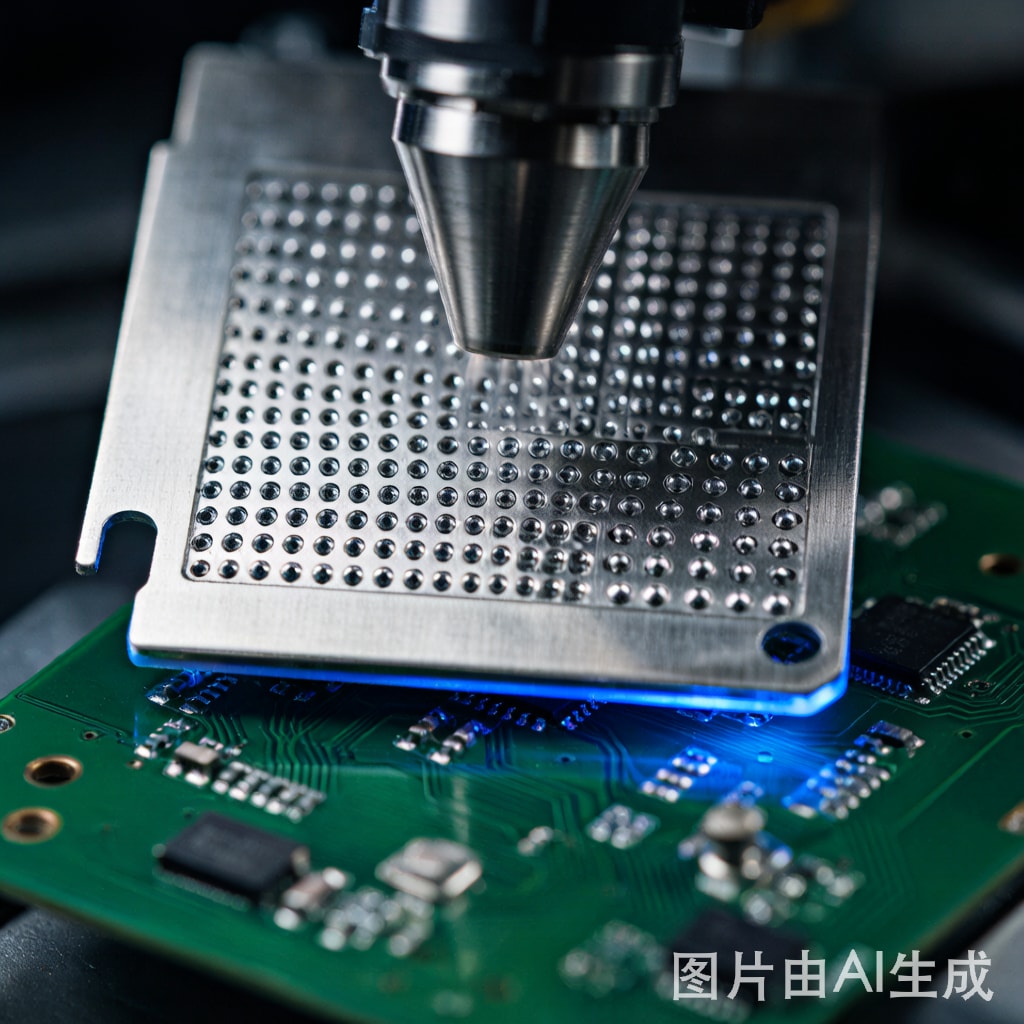
Component Removal
Per IPC-7711/7721, BGA removal uses controlled hot air convection or infrared heating to bring the entire component to reflow temperature without exceeding the package’s maximum rated temperature (typically 245-260°C peak for lead-free SAC BGAs). The standard procedure is:
Step 1: Pre-Heating
- Bottom-side preheat to 100-150°C using the rework station’s bottom heater
- Top-side preheat ramp at 1-2°C/second to 150°C soak temperature
- Soak at 150-180°C for 60-90 seconds to equalize temperature across the package
Step 2: Reflow
- Ramp from soak to peak temperature of 240-245°C at 1-2°C/second
- Time above liquidus (TAL) of 45-75 seconds for SAC alloys
- Peak temperature measured at the BGA package body, not the air stream
Step 3: Lift-Off
- Once peak temperature is reached and the solder is fully molten, a vacuum pickup lifts the BGA straight up with minimal lateral force
- Lateral movement during lift can scrape pads or lift traces — keep motion purely vertical
- Allow the component to cool naturally on the pickup or on a heat-resistant surface
Site Preparation
After component removal, the PCB land pads require cleaning before a new component can be placed. Residual solder, flux residue, and lifted pads must be addressed:
Solder Removal
- Apply flux to the pad area
- Use a solder sucker or desoldering braid to remove residual solder from each pad
- Alternatively, use a specialized BGA pad cleaning iron with a shaped tip that matches the pad array pattern
- Target condition: flat, shiny copper pads with no solder residue or bridging
Pad Inspection
- Inspect each pad under 10-30× magnification for lifted pads, missing pads, or damaged solder mask
- Damaged pads: IPC-7711/7721 describes repair procedures for lifted pads, including adhesive-backed replacement pads
- Stub trace repair: if a pad is missing, the co
ecting trace can be carefully scraped and a small wire added to restore the co
ection
Cleaning
- Clean the area with isopropyl alcohol or a compatible defluxer
- Remove all flux residue to enable proper wetting during the new component’s reflow
- Inspect under UV light to verify no fluorescent residue remains
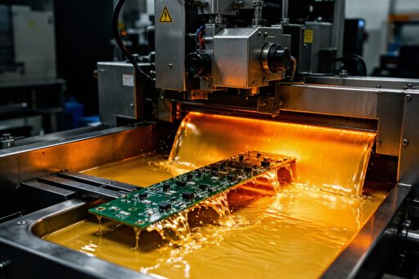
BGA Reballing Methods
When the removed BGA will be re-used, it must be reballed — the original solder balls are removed and new spheres of the correct alloy and size are applied. Three common methods exist:
Stencil Method (Most Common)
- Apply solder paste to the cleaned BGA pads using a laser-cut stainless steel stencil matched to the ball grid pattern
- Reflow the paste in a controlled atmosphere oven or on a hot plate to form uniform solder spheres
- Advantage: low equipment cost, suitable for low-to-medium volume reballing
- Disadvantage: sphere diameter control depends on paste volume consistency, typically ±10% on diameter
Pre-Formed Sphere Method
- Apply flux to the BGA pads
- Place pre-formed solder spheres using a vibrating fixture, vacuum jig, or manual placement under microscope
- Reflow to attach the spheres to the pads
- Advantage: best diameter uniformity (±5 µm typical), matches original ball geometry
- Disadvantage: requires a sphere placement fixture matched to each BGA pattern; higher equipment investment
Direct Sphere Application
- Specialized equipment dispenses individual spheres directly onto each pad
- Used primarily in semiconductor packaging and high-volume reballing operations
- Highest precision but rarely justified for SMT-level rework
Replacement Component Placement and Reflow
- Apply solder paste or flux to the cleaned PCB pads (flux-only for reballed components, paste for new components)
- Use a split-vision alignment system to position the new BGA precisely over the pads, with typical placement accuracy of ±50 µm
- Reflow using a profile matched to the new component’s specifications and the board’s thermal mass
- Cool the assembly under controlled conditions to avoid thermal shock
Acceptance Criteria and Verification
IPC-7711/7721 specifies acceptance criteria for reworked BGAs based on the assembly’s performance class:
- Class 1: Functional verification only; cosmetic defects acceptable as long as electrical function is preserved
- Class 2: Visual inspection for obvious defects (bridging, missing balls, gross misalignment); X-ray inspection recommended for hidden joints
- Class 3: 100% X-ray inspection of all reworked joints, with void limits and joint geometry requirements matching original assembly standards
For all classes, electrical testing (flying probe, in-circuit test, or boundary scan) is required to confirm continuity and isolation. Functional testing should also be performed to verify the reworked assembly operates within specification.
Conclusion
BGA rework per IPC-7711/7721 is a precise, multi-step process requiring specialized equipment, careful process control, and rigorous verification. The procedure is most valuable for engineering prototypes, low-volume production, and high-value assemblies where component-level repair is more economical than board replacement. Success depends on moisture management before rework, controlled thermal profiles during component removal and replacement, thorough site preparation, and verification through X-ray inspection and electrical testing. With proper training and equipment, BGA rework can achieve reliability comparable to original assembly, extending the service life of high-value electronics.