The Thermal Bottleneck in Conventional PCB Construction
Standard FR4 laminate has a thermal conductivity of approximately 0.3–0.4 W/m·K—three orders of magnitude lower than copper (385 W/m·K). When a high-power component (BGA IC, power MOSFET, LED array) dissipates 5–50W on a conventional PCB, the heat must traverse this low-conductivity FR4 barrier to reach a heatsink on the opposite side. The result is a significant thermal bottleneck that limits the power density of the design and forces either larger heatsinks, forced-air cooling, or reduced component performance.
Thermal via arrays—the traditional solution—help by providing copper cylinders that conduct heat through the FR4. However, a via is limited by its small cross-sectional area: a 0.3 mm diameter via with 25 μm plating has an effective copper cross-section of only 0.024 mm², and a typical 5×5 via array provides a total thermal conductance of approximately 0.5–2.0 W/K. For components dissipating more than 10W, even large via arrays ca
ot provide adequate thermal conductance.
Embedded copper coin technology solves this bottleneck by replacing the via array with a solid copper cylinder or block embedded directly in the PCB laminate, providing a thermal conductance 20–100× higher than via arrays at the same footprint area.
What Is Embedded Copper Coin Technology?
Basic Concept
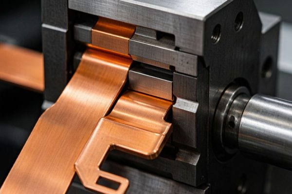
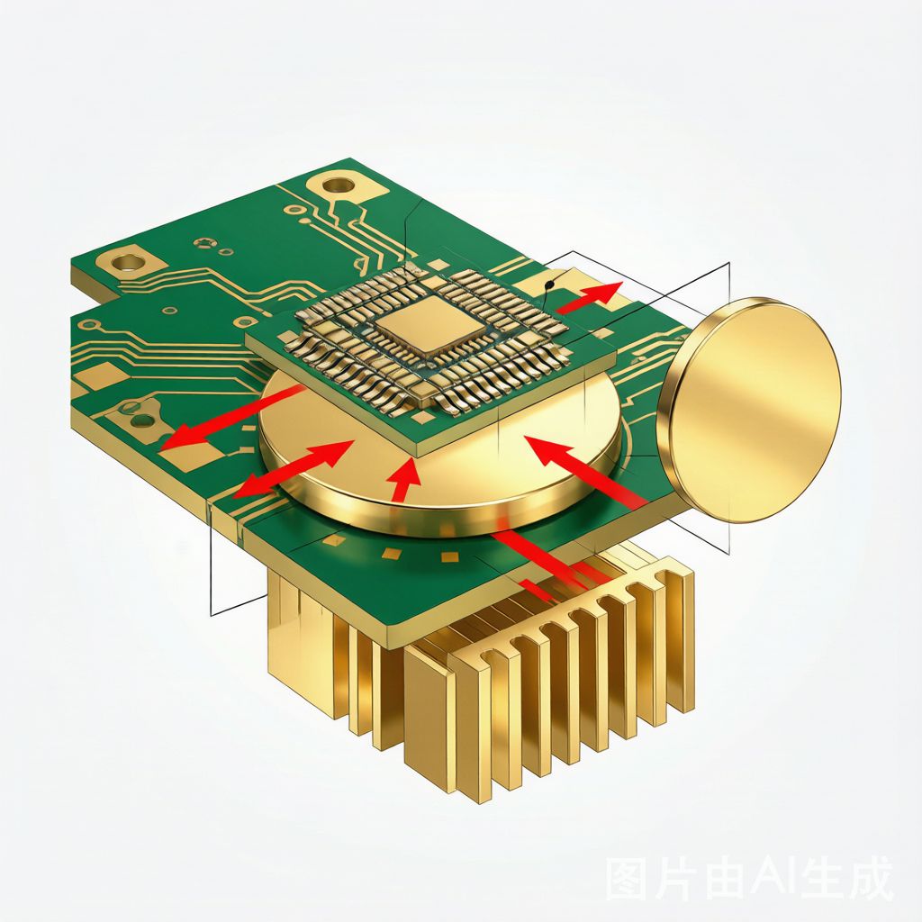
An embedded copper coin is a thick (1.0–5.0 mm) solid copper piece that is inserted into a routed cavity in the PCB laminate during fabrication. The coin is bonded to the surrounding FR4 by prepreg adhesive under lamination pressure, creating a monolithic copper heat path from the component solder pads on the top surface to the heatsink contact area on the bottom surface.
The coin can be a simple cylindrical or rectangular plug (for single-component cooling) or a larger shaped block that serves multiple components simultaneously. Some designs integrate copper coins with internal cha
els for liquid cooling, though this requires multi-step fabrication and is reserved for ultra-high-power applications (≥100W).
Thermal Conductance Comparison
For a 15 mm × 15 mm footprint (typical large BGA pad):
- Via array (25 × 0.3mm vias, 25μm plating): Thermal conductance ≈ 1.5 W/K. Temperature drop across PCB: 10–20°C at 15W dissipation.
- Copper coin (15 × 15 × 2.0 mm solid copper): Thermal conductance ≈ 52 W/K (385 W/m·K × 225 mm² / 2.0 mm). Temperature drop across PCB: 0.3°C at 15W dissipation.
- Improvement factor: 35× higher thermal conductance with the copper coin versus the via array.
This dramatic improvement means that components previously requiring large external heatsinks and forced-air cooling can now be cooled with modest heatsinks and natural convection, reducing product size, weight, and cost.
Design Rules for Embedded Copper Coin PCBs
Coin Sizing and Placement
The coin should extend at least 2 mm beyond the component thermal pad on all sides to provide adequate heat spreading. For a BGA with a 10 mm × 10 mm thermal pad, the minimum coin size is 14 mm × 14 mm. Larger coins provide better heat spreading but consume more board area and increase cost.
The coin thickness should span the full PCB thickness when possible, creating a direct thermal path from top to bottom. If the PCB is 2.0 mm thick, use a 2.0 mm coin. Partial-thickness coins (e.g., 1.5 mm in a 2.0 mm board) are possible but leave an FR4 gap at one surface that adds thermal resistance.
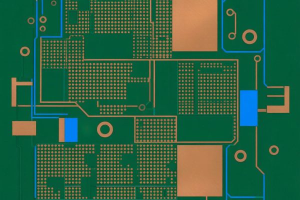
Coin-to-Trace Interface Design
At the top surface, the coin is exposed as a copper pad that the component solder joints directly contact. Design rules for this interface:
- Solder mask opening: The solder mask must be opened over the entire coin area. Use a solder mask opening 0.1–0.2 mm larger than the coin on all sides to ensure complete exposure.
- Surface finish: Apply ENIG (3–5 μm Ni / 0.05 μm Au) or OSP over the coin surface. ENIG is preferred for high-reliability applications because gold provides excellent solderability and the nickel barrier prevents copper-tin intermetallic overgrowth during reflow.
- Trace routing around coins: No signal traces should route over the coin area—they will be cut when the cavity is routed. Route all traces around the coin perimeter with a minimum 0.2 mm clearance from the coin edge.
- Ground plane co
ection:
Coect the coin to the ground plane on both top and bottom layers. This prevents the coin from acting as a floating conductor that could accumulate static charge or interfere with signal integrity.
Structural Considerations
Embedded copper coins create a localized stiffness mismatch in the PCB. Copper is harder and stiffer than FR4, which means the coin area acts as a rigid island surrounded by a more flexible laminate. This mismatch can cause two problems:
- Warpage during lamination: The copper coin area expands less than the surrounding FR4 during the lamination heat cycle (copper CTE ≈ 17 ppm/°C vs. FR4 CTE ≈ 14 ppm/°C in-plane), potentially causing local warpage. Coins larger than 25 mm × 25 mm may require a symmetric counter-bore on the opposite side to maintain board flatness.
- Vibration stress concentration: In high-vibration applications (automotive, aerospace), the stiffness boundary between the coin and FR4 creates a stress concentration. Add 4–8 mechanical mounting holes near the coin perimeter to anchor the board to the chassis, distributing the vibration load.
Manufacturing Process for Embedded Copper Coin PCBs
Step-by-Step Fabrication
- I
er layer etching:
Etch ier layer copper patterns (ground planes, power planes) as normal. The coin cavity area is left as solid copper on these layers.
- Cavity routing: After i
er layer lamination, route the coin cavity through the top portion of the laminate stackup using CNC milling. The cavity depth equals the coin thickness minus the top copper foil thickness (typically 0.035 mm for 1 oz foil). Cavity tolerance: ±0.05 mm on depth, ±0.1 mm on X-Y dimensions.
- Coin insertion: Insert the pre-machined copper coin into the cavity. The coin should fit with 0.05–0.15 mm clearance on all sides—too tight prevents prepreg flow; too loose reduces bonding strength and allows coin shift during lamination.
- Prepreg fill: Place prepreg sheets over the coin and surrounding laminate. The prepreg flows into the coin-to-laminate gap during lamination, bonding the coin to the board. Use a high-flow prepreg (e.g., 1080 or 2116 style) to ensure complete gap filling.
- Outer layer lamination: Laminate the outer layer copper foil and prepreg under standard press conditions (180°C, 300 psi, 60 minutes). The prepreg bonds the coin to the surrounding laminate and the outer foil to the board surface.
- Outer layer patterning: Photoimage and etch the outer layers. The coin area appears as a solid copper pad—no etching is needed within the coin footprint. Route traces around the coin perimeter.
- Solder mask and surface finish: Apply solder mask and surface finish (ENIG, OSP, etc.) as normal. The coin surface receives the same finish as all other exposed copper areas.
Manufacturing Cost Impact
Embedded copper coins add cost through three mechanisms: the coin material itself, the CNC cavity routing step, and the additional lamination complexity. Typical cost impact:
- Single coin (15 × 15 × 2.0 mm): Adds $0.50–1.00 to the board cost (coin material $0.10, routing $0.30–0.60, lamination yield impact $0.10–0.30).
- Multiple coins (4 coins per board): Adds $2.00–4.00 per board.
- Yield impact: CNC routing and coin insertion have a combined yield of 95–98%. Most yield loss comes from coin shift during lamination or incomplete prepreg fill causing delamination.
For a board with a $30–50 baseline cost, adding copper coins represents a 3–8% cost increase—a modest investment compared to the alternative of larger heatsinks, fans, and thermal interface materials that might add $5–15 to the total product BOM.
Thermal Performance Case Studies
Case 1: 15W BGA Processor
A 15W BGA processor on a 2.0 mm 4-layer PCB:
- Without copper coin (via array only): Junction-to-ambient thermal resistance: 25°C/W. At 15W, junction temperature rises to 75°C above ambient. Requires a 40 mm × 40 mm extruded heatsink with forced-air cooling.
- With 15 × 15 × 2.0 mm copper coin: Junction-to-ambient thermal resistance: 8°C/W. At 15W, junction temperature rises to only 24°C above ambient. A 25 mm × 25 mm flat heatsink with natural convection is sufficient.
- Result: 68% reduction in thermal resistance, elimination of fan cooling, 40% heatsink size reduction.
Case 2: 30W Power MOSFET Array
Four 7.5W power MOSFETs on a single 25 × 25 mm copper coin:
- Without coin: Each MOSFET junction reaches 110°C at 7.5W, requiring individual heatsinks and thermal pads per device.
- With shared copper coin: The coin spreads heat from all four devices to a single heatsink contact area. Junction temperatures drop to 70°C at 7.5W per device. One heatsink replaces four.
- Result: Simplified thermal solution, reduced component count, lower assembly cost.
When to Use Copper Coins vs. Alternatives
Embedded copper coins are most effective when:
- Component power dissipation exceeds 5W per device and via arrays ca
ot provide adequate thermal conductance.
- The product form factor prohibits large external heatsinks (embedded devices, sealed enclosures).
- The PCB is 1.6–3.2 mm thick, allowing a full-thickness coin that spans the board.
- Only 1–4 high-power components need enhanced cooling—the rest of the board operates at normal power levels.
Alternatives are preferable when: many low-power devices need modest cooling improvement (use heavy copper layers), power exceeds 50W per device (use copper coin + liquid cooling or external heatsink), or the PCB is too thin (<1.0 mm) for coin embedding (use copper foil stackup or metal-core PCB).
Conclusion
Embedded copper coin technology transforms the PCB from a thermal barrier into a thermal conductor by replacing low-conductivity FR4 with solid copper in the critical heat path area. The 20–100× thermal conductance improvement over via arrays enables higher power density, smaller heatsinks, and simpler cooling solutions—all at a modest 3–8% board cost increase. For electronics products destined for compact, sealed, or fanless enclosures, copper coin embedding is a design enabler that makes thermal performance possible rather than merely marginal. The key to successful implementation lies in proper coin sizing, careful cavity routing, and adequate prepreg bonding—all well-established PCB fabrication capabilities at most leading fabricators.