The Hidden Cost of Lead-Free Wave Soldering
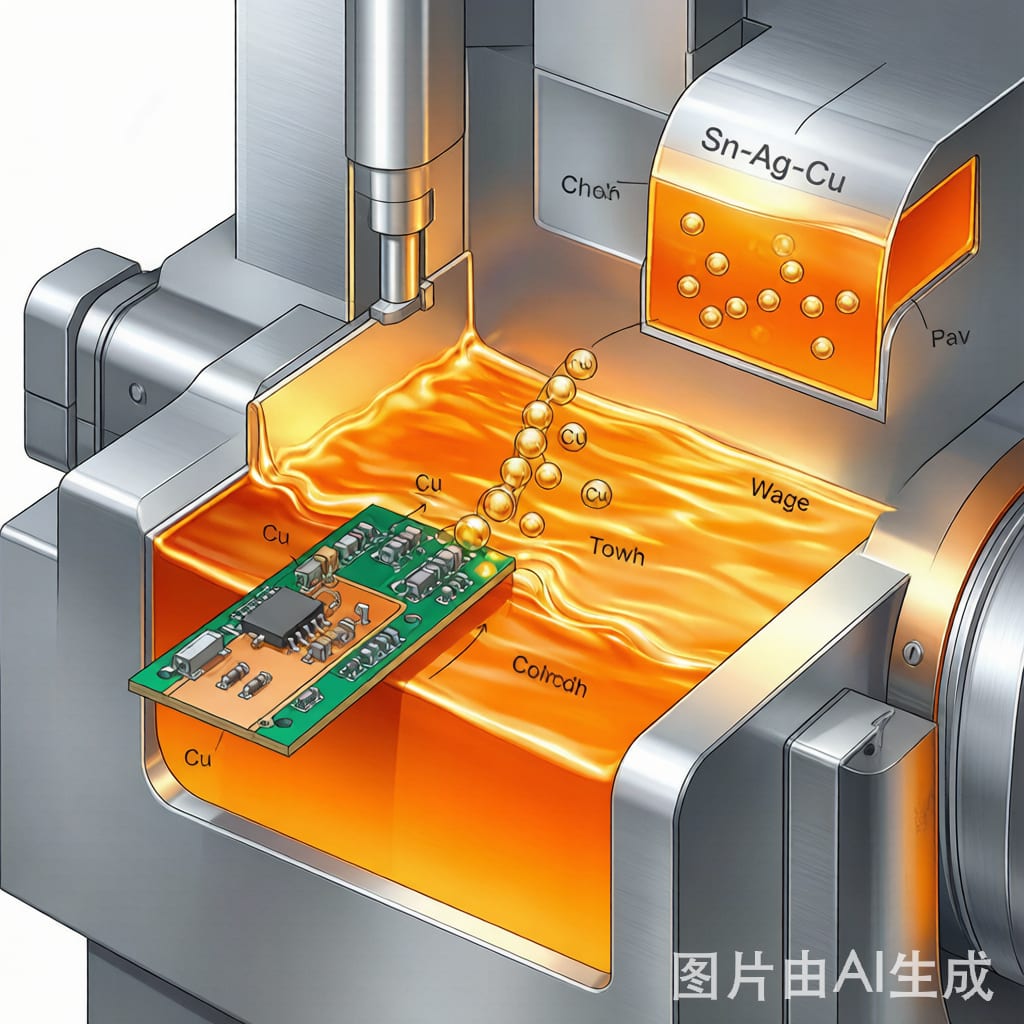
When a PCB passes through a wave soldering machine, the molten solder wave contacts every exposed copper surface on the bottom side of the board—through-hole component leads, via barrels, and exposed copper pads. Copper dissolves into the molten solder at a rate that depends on temperature, solder alloy composition, and contact time. In the SnPb era, copper dissolution was a manageable concern because Sn63/Pb37 solder has a relatively low tin content (63%) and a modest copper solubility limit. The transition to SAC305 (96.5% Sn, 3.0% Ag, 0.5% Cu) changed the equation dramatically.
SAC305 contains 96.5% tin, and pure tin has an extremely high affinity for copper. At typical wave soldering temperatures of 255–265°C, copper dissolves into SAC305 at rates of 0.5–1.5 μm per second of contact—2–4× faster than in SnPb solder. Over months of continuous production, this dissolved copper accumulates in the solder pot, eventually exceeding the solubility limit and forming brittle Cu₆Sn₅ intermetallic particles that degrade solder joint quality and reliability.
The Science of Copper Dissolution in SAC Alloys
Dissolution Rate and Temperature Dependence
Copper dissolution in molten tin-based solder follows an Arrhenius relationship—the rate approximately doubles for every 20°C increase in temperature. At 250°C, the dissolution rate of copper in SAC305 is approximately 0.5 μm/s; at 265°C, it increases to 1.2 μm/s; and at 280°C, it reaches 2.5 μm/s. This temperature sensitivity means that even a 5°C increase in pot temperature can accelerate copper contamination by 20–30%.
The dissolution rate also depends on the local tin concentration at the copper-solder interface. Fresh solder (with low copper content) dissolves copper faster than copper-saturated solder. This creates an interesting dynamic: a freshly charged solder pot initially dissolves copper rapidly, but as copper accumulates and the solder approaches saturation, the dissolution rate decreases.
Copper Solubility Limit in SAC305
At 260°C, the maximum copper solubility in SAC305 is approximately 1.5% by weight (15,000 ppm). Above this concentration, copper precipitates as Cu₆Sn₅ intermetallic crystals. These needle-shaped intermetallics (10–50 μm long, 1–5 μm diameter) are brittle and can act as stress concentrators in solder joints, reducing thermal cycling life by 30–50%.
IPC J-STD-001 specifies a maximum copper contamination level of 0.8% (8,000 ppm) for SnPb solder and 1.0% (10,000 ppm) for lead-free solder—well below the solubility limit to provide a safety margin against intermetallic precipitation.
Impact of Copper Contamination on Solder Joint Quality
Viscosity and Wetting Changes
As copper content increases from 0.5% to 1.0%, the solder viscosity increases by approximately 15–20%. This manifests as slower wetting speeds, reduced solder capillary flow in through-holes, and increased incidence of insufficient hole-fill on thick PCBs. Solder joints may appear grainy or dull rather than smooth and shiny, although this cosmetic change does not necessarily indicate a reliability problem.
Intermetallic Precipitation
When copper exceeds the solubility limit, Cu₆Sn₅ intermetallic particles form throughout the solder volume. In through-hole joints, these particles can concentrate at the copper-solder interface, thickening the intermetallic layer and creating a brittle fracture plane. Thermal cycling tests show that joints with thick intermetallic layers (≥5 μm) fail at 40–60% fewer cycles than joints with normal IMC thickness (1–3 μm).
Freezing Point Depression and Reflow Issues
Excess copper in the solder alters the liquidus temperature. A SAC305 pot with 1.2% copper has a liquidus approximately 3–5°C higher than fresh solder, which can cause incomplete wetting on thermal-mass-heavy assemblies where the board temperature may not reach the required superheat.
Estimating Solder Pot Contamination Rate
The rate of copper accumulation in a wave solder pot depends on three factors: production volume, board copper content, and pot temperature. A practical estimation method:
- Typical copper exposure per board: For a double-sided PCB with 200 through-hole component leads and 150 vias, the total exposed copper surface area is approximately 200–400 mm² per board.
- Dissolution per board: At 260°C with 3–5 seconds of wave contact per side, approximately 1.5–3.0 μm of copper dissolves from each exposed surface. This translates to roughly 0.5–2.0 mg of copper per board.
- Pot accumulation: In a 300 kg solder pot ru
ing 500 boards per day, the daily copper accumulation is 0.25–1.0 g, or approximately 0.8–3.3 ppm per day. It takes 3,000–12,000 days to reach the 10,000 ppm limit from fresh solder—far longer than the typical pot change interval.
However, this calculation assumes that the solder pot is not exposed to other copper sources. In practice, copper jigs, fixtures, and especially copper pallet carriers can contribute significant additional copper. A single copper pallet carrier partially immersed in the solder wave can dissolve 50–200 mg of copper per day—equivalent to 100–400 boards worth of dissolution.
Contamination Control Strategies
1. Regular Copper Analysis
Test the solder pot copper content weekly using ICP-OES (inductively coupled plasma optical emission spectroscopy) or XRF (X-ray fluorescence). Most wave soldering equipment vendors offer pot analysis services, and portable XRF analyzers can provide results within minutes at the production floor level. Track results on an SPC chart with upper and lower control limits at 0.8% and 0.3% copper respectively.
2. Solder Pot Partial Replacement
When copper content exceeds 0.8%, replace 20–30% of the pot volume with fresh SAC305 alloy. This dilutes the copper concentration back below the control limit. The replacement solder should be pre-heated to minimize thermal shock to the pot. Some facilities schedule quarterly partial replacements as a preventive measure.
3. Temperature Optimization
Operate the wave solder pot at the minimum temperature that provides acceptable hole-fill. For most SAC305 applications, 255–260°C is sufficient. Reducing the pot temperature from 265°C to 255°C decreases the copper dissolution rate by approximately 40%, significantly extending pot life.
4. Non-Copper Fixtures
Replace copper and brass pallet carriers, jigs, and fingers with titanium or stainless steel alternatives. Titanium has negligible solubility in SAC305 at wave soldering temperatures, and stainless steel dissolution rates are approximately 100× lower than copper.
5. Contact Time Minimization
Optimize the conveyor speed and wave configuration to minimize the time each board spends in contact with the solder wave. A contact time of 3–5 seconds per side is typically sufficient for good hole-fill on boards up to 3.2 mm thickness. Longer contact times provide diminishing wetting improvement while linearly increasing copper dissolution.
Practical Pot Life Guidelines
| Production Volume | Pot Size | Estimated Pot Life | Recommended Action |
|---|---|---|---|
| Low (≤200 boards/day) | 200–300 kg | 18–24 months | A
ual analysis, replace at 0.8% Cu |
| Medium (200–800 boards/day) | 300–500 kg | 12–18 months | Quarterly analysis, partial replace if needed |
| High (≥800 boards/day) | 500–800 kg | 8–12 months | Monthly analysis, scheduled partial replacement |
Conclusion
Copper dissolution in lead-free wave soldering is an inevitable process that must be managed rather than prevented. The key control parameters are pot temperature, copper analysis frequency, and fixture material selection. By operating at the minimum effective temperature, using non-copper fixtures, and monitoring copper content regularly, SMT manufacturers can maintain solder pot chemistry within IPC limits and achieve consistent joint quality throughout the pot’s service life. The cost of regular analysis and periodic partial solder replacement is negligible compared to the cost of field failures caused by intermetallic-contaminated solder joints.