The Thermal-RF Trade-off in Shielding Can Design
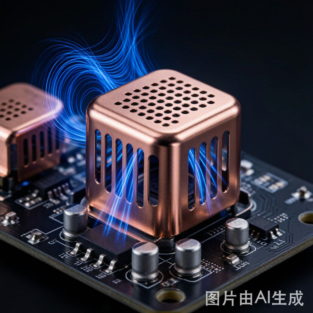
EMI shielding cans serve a dual purpose: they suppress radiated electromagnetic interference from high-speed digital circuits, and they trap heat. Without ventilation, components inside a fully sealed shield can operate 15–30°C hotter than exposed equivalents—a temperature delta that can halve the MTBF of power management ICs and RF power amplifiers. This creates a direct engineering trade-off: larger ventilation openings improve airflow and reduce junction temperatures, but degrade RF shielding effectiveness (SE) by allowing electromagnetic energy to leak through the apertures.
This article covers the physics of aperture-based shielding leakage, practical ventilation pattern design, and how to strike the optimal thermal-RF balance for SMT shield cans.
Aperture Waveguide Theory: How Holes Leak RF Energy
A ventilation hole in a shielding can acts as a waveguide below cutoff. Below the cutoff frequency, electromagnetic fields attenuate exponentially as they pass through the aperture. The degree of attenuation is given by the aperture’s cutoff frequency (fc), which depends on the hole geometry:
- Circular hole: fc = 175.8 / d (GHz·mm), where d is the diameter in millimeters. A 3 mm circular hole has fc ≈ 58.6 GHz.
- Rectangular slot: fc = 150 / w (GHz·mm), where w is the longest dimension. A 5 mm slot has fc ≈ 30 GHz.
Below fc, the shielding effectiveness (SE) contributed by the aperture is approximately: SE(dB) = 27.3 × (t / d) for circular holes, where t is the material thickness and d is the diameter. For a typical 0.2 mm thick stainless steel shield can with 3 mm diameter vent holes, this works out to approximately 1.8 dB of aperture attenuation—essentially negligible for microwave frequencies but adequate for sub-1 GHz applications.
Ventilation Pattern Parameters and Their Impact on SE
Hole Size vs. Shielding Frequency Range
- ≤1 mm diameter: Maintains SE above 40 dB for frequencies up to 10 GHz. Excellent for 5G sub-6 GHz and Wi-Fi 6E shielding. Airflow is significantly restricted.
- 1.5–2.5 mm diameter: Balanced option for frequencies up to 3–6 GHz. Moderate airflow, suitable for general digital circuit shielding.
- 3–5 mm diameter: Good airflow but SE degradation becomes significant above 1 GHz. Use only when thermal constraints are dominant and radiated emissions are in lower frequency bands.
Hole Spacing and Array Effects
When multiple holes are placed in an array, the total SE degradation is not simply additive. Closely spaced holes (center-to-center spacing < 2× diameter) couple electromagnetically, reducing the effective SE more than isolated holes of the same size. The worst case is a regular grid pattern, where constructive interference between adjacent apertures can reduce SE by an additional 3–6 dB compared to isolated apertures of the same total open area.
Best practice: maintain center-to-center spacing ≥ 3× hole diameter, and consider staggered (hexagonal) patterns instead of square grids. Staggered patterns distribute the apertures more evenly and reduce coupling while maintaining the same open-area ratio.
Open-Area Ratio Targets
The open-area ratio (total hole area / total shield surface area) determines both airflow capacity and SE performance:
- 10–15% open area: Minimal thermal benefit, excellent SE. For components with ≤1W dissipation.
- 20–30% open area: Good thermal-RF balance. Suitable for most digital and mixed-signal circuits.
- 35–50% open area: Maximum thermal performance, significant SE compromise. Use only with additional SE margin or for low-frequency shielding requirements (below 500 MHz).
Thermal CFD Considerations
While the open-area ratio is a useful first-order metric, thermal performance depends on more than just total hole area. CFD (computational fluid dynamics) studies reveal several important insights:
- Inlet-outlet pairing matters: Ventilation on opposing faces of the shield can creates a chimney effect that doubles convective airflow compared to single-face perforation.
- Hole distribution trumps total area: Uniformly distributed small holes provide better cooling than concentrated large holes, because they create more distributed flow paths that sweep across all components.
- Standoff height effect: The gap between the shield can wall and PCB (typically 0.1–0.2 mm for standard SMT attachment) provides negligible airflow. Increasing standoff to 0.5–1.0 mm significantly improves natural convection.
- Top-surface perforation: Holes on the top face of the shield can are more effective for thermal management than side-wall holes, as they allow the natural vertical convection plume to exit unimpeded.
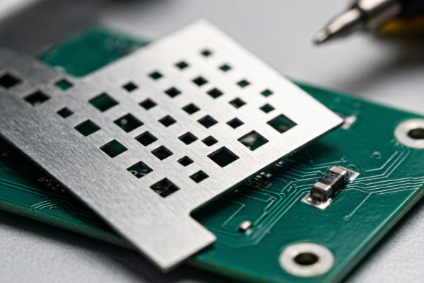
Advanced Ventilation Techniques
Frequency-Selective Surface (FSS) Patterns
For applications requiring both high airflow and high SE at specific frequency bands, FSS patterns etched into the shield can provide bandpass or bandstop filtering. A Jerusalem cross FSS pattern, for example, can achieve 30+ dB attenuation at a target frequency (e.g., 2.4 GHz Wi-Fi) while maintaining 60% open area for airflow. FSS adds cost and requires precision manufacturing (chemical etching or laser cutting), limiting it to high-value applications like military radios and satellite transceivers.
Multi-Layer Shield Cans
A dual-layer shield with offset ventilation patterns—similar to a double-pane window—can simultaneously achieve high airflow and high SE. The i
er and outer layers have identical hole patterns but are offset by half a pitch. Electromagnetic waves passing through the outer holes encounter the i
er solid surface, forcing the field to propagate laterally within the gap before finding an i
er hole to exit. The lateral propagation path adds significant attenuation above 2 GHz while maintaining unimpeded airflow.
Design Guidelines Summary
- For components dissipating ≤2W: 1.5 mm diameter vent holes, 20% open area, circular staggered pattern. Maintains good SE up to 5 GHz.
- For components dissipating 2–5W: 2.0 mm diameter holes, 25–30% open area, top-face perforation with side-wall inlets. Consider increasing shield can height by 1–2 mm to improve chimney effect.
- For components dissipating >5W: 2.5 mm holes, 30–35% open area, ventilation on three faces (top + two opposing sides). Evaluate whether SE margin allows larger apertures or whether a heatsink-attached shield is more appropriate.
- For >10 GHz shielding: limit all apertures to ≤1 mm diameter regardless of thermal requirements. Use a shield-integrated heatsink or supplemental cooling (fan, thermal pad to chassis) to manage thermal load.
Conclusion
EMI shield can ventilation design is a classic multi-physics optimization problem. The aperture waveguide model provides the RF framework, while CFD analysis handles the thermal side. For most commercial electronics, a 1.5–2.5 mm hole diameter with 20–30% open area and staggered pattern delivers the best thermal-RF balance. When in doubt, thermal simulation paired with pre-compliance EMC sca
ing of a prototype shield can will resolve the trade-off definitively and avoid the cost of over-designing either parameter.