The Inspection Triad: AOI, SPI, and X-Ray in Modern SMT Lines
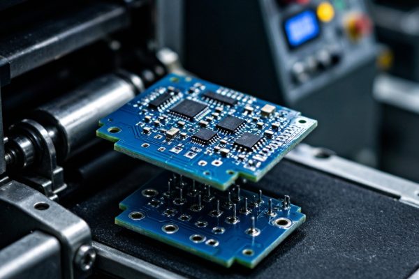
In a high-mix SMT production line placing components ranging from 0201 passives to 1,500+ ball BGAs, no single inspection technology covers all defect modes. The modern approach combines three complementary systems: Solder Paste Inspection (SPI) before component placement, Automated Optical Inspection (AOI) after reflow, and X-ray inspection for hidden joints. This article compares the capabilities, resolution limits, and ROI of each technology.
Solder Paste Inspection: Catching Defects at the Source
SPI systems use structured light projection—typically Moiré interferometry or laser triangulation—to measure solder paste deposits immediately after stencil printing. A 3D SPI system captures deposit volume, area, height, and XY offset for every pad on the board.
What SPI Detects (and Why It Matters)
- Insufficient paste volume: Below 50% of nominal, the risk of opens and head-in-pillow on BGAs rises exponentially. SPI catches this before components are placed, enabling paste-on-paste reprint or stencil cleaning.
- Paste bridging: For 0.4 mm pitch QFPs, a bridge as small as 50 μm between adjacent pads can survive reflow and create a short. SPI resolution of 10–15 μm per pixel in Z-axis easily resolves this.
- Paste slump/smear: After multiple print cycles without cleaning, paste can smear under the stencil, increasing pad-to-pad bridging risk.
- Stencil clogging trends: SPI statistical process control (SPC) data reveals which apertures are progressively clogging, enabling predictive stencil cleaning intervals.
Industry data shows that SPI with closed-loop feedback to the printer reduces end-of-line defect rates by 40–60% compared to lines without SPI. The economics are compelling: catching a paste defect at SPI costs pe
ies, while catching the same defect as a reflowed short at AOI costs dollars in rework.
Automated Optical Inspection: The Post-Reflow Gatekeeper
AOI systems capture high-resolution 2D images of assembled PCBs and compare them against a golden board reference or CAD-derived tolerance model. Modern 3D AOI adds structured light or laser profiling to measure component coplanarity, solder fillet height, and lifted lead detection.
2D AOI vs 3D AOI: Choosing the Right Capability
2D AOI uses multi-angle colored LED illumination and high-resolution cameras (12–25 MP) to detect:
– Component presence, polarity, and correct part number (OCR)
– Solder joint wetting quality via reflected light pattern analysis
– Bridging between adjacent pads
– Component offset and rotation
3D AOI adds height information, critical for detecting:
– Lifted leads on gull-wing packages
– BGA/CSP coplanarity issues (ball height variation)
– Tombstoned components (one end lifted)
– Insufficient solder fillet height on J-lead and gull-wing joints
The resolution requirement scales with component size. For 0201 passives (0.6 × 0.3 mm), inspection requires at minimum 10 μm/pixel resolution. For 01005 components, 5 μm/pixel is needed. For solder joint inspection on 0.4 mm pitch BGAs, 3D AOI with laser triangulation provides reliable coplanarity measurement.
AOI Programming and False-Call Rate
The biggest operational challenge with AOI is the false-call rate—the percentage of flagged defects that are actually acceptable. A well-tuned AOI program runs at 5–10% false-call rate; a poorly tuned one can exceed 40%, overwhelming manual verification stations and eroding operator trust. CAD-based programming with intelligent component libraries reduces initial programming time from days to hours while improving first-pass yield.
X-Ray Inspection: Seeing the Invisible
X-ray inspection is essential for solder joints hidden beneath component bodies: BGA balls, QFN thermal pads, PoP (Package-on-Package) bottom-layer joints, and press-fit co
ector pins. Two configurations dominate SMT lines.
2D X-Ray (Transmission)
A 2D X-ray system passes X-rays through the PCB onto a flat-panel detector. Dense materials (solder, copper) absorb more radiation and appear darker. 2D X-ray detects:
– BGA voids (≥10% of ball diameter per IPC-7095 Class 2)
– Solder bridging under BGAs and QFNs
– Insufficient solder on BGA balls (reduced diameter)
– Missing balls in the i
er array (not detectable by AOI)
3D X-Ray (Computed Tomography – CT)
3D X-ray rotates the board through multiple angles and reconstructs a volumetric model using computed tomography algorithms. Individual BGA ball slices can be examined at any plane. CT X-ray adds:
– Head-in-pillow detection (partial contact without metallurgical wetting)
– Void location relative to the ball-pad interface (edge voids near the pad are more detrimental than center voids)
– Multi-layer BGA and PoP joint inspection
– Copper trace integrity beneath BGA packages
The cost differential is significant: a 2D inline X-ray system runs US$100,000–200,000, while 3D CT systems range from US$250,000–600,000. For most contract manufacturers, 2D inline X-ray with offline 3D CT for failure analysis provides the best ROI.
Choosing the Right Inspection Mix
The optimal inspection strategy depends on product complexity and reliability requirements:
- Consumer electronics (smartphones, tablets): 3D SPI + 3D AOI at line speed, offline 2D X-ray sampling for BGAs. Throughput is the priority.
- Automotive (under-hood ECUs, ADAS): 3D SPI + 3D AOI + inline 2D X-ray for 100% BGA inspection. Zero-escape mentality.
- Aerospace/defense/medical: 3D SPI + 3D AOI + inline 2D/3D X-ray with 100% inspection. Additional offline CT X-ray for first-article and lot sampling.
- Industrial controls: 3D SPI + 2D AOI with selective 3D for critical components. Offline 2D X-ray for QFN and BGA audits.
Conclusion
SPI, AOI, and X-ray are not competing technologies—they are complementary inspection layers that together form a comprehensive defect-detection strategy. The investment case is straightforward: the cost of one field return from an undetected defect typically exceeds the a
ual depreciation of all three inspection systems combined. In today’s SMT environment, you ca
ot inspect quality into a product—but you can certainly detect when it isn’t there.