The Role of Copper Busbars in Modern Electronics
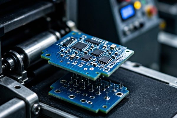
As power electronics push toward higher current densities—EV traction inverters switching at hundreds of amps, AI server motherboards with 600+ A peak demands, and renewable energy inverters operating at 1500 V DC—traditional PCB copper weight reaches its practical limits. At current levels above 50–100 A, the wide traces and heavy copper required to carry load current on a PCB become mechanically fragile, thermally constrained, and uneconomical. Copper busbars emerge as the standard solution: solid or laminated copper conductors that handle high currents with minimal voltage drop and excellent thermal management.
This guide covers the engineering decisions behind copper busbar selection, sizing, and integration with SMT-assembled PCBs in power electronics applications.
Busbar Material Selection
Pure Copper (C11000 / ETP Copper)
Standard electrolytic tough pitch (ETP) copper, designated C11000, is the dominant busbar material. With electrical conductivity of 101% IACS (International A
ealed Copper Standard) at 20°C and excellent formability, C11000 is suitable for most power electronics busbar applications.
- Conductivity: 5.96 × 10⁷ S/m (101% IACS)
- Tensile strength: 220–250 MPa (a
ealed), 350–400 MPa (hard temper)
- Cost: Most economical option
- Limitations: Susceptible to oxidation; requires plating for solderable or high-humidity environments
Copper Alloys for High-Strength Applications
For applications requiring spring contact force or vibration resistance, copper alloys offer higher mechanical strength at the cost of conductivity:
| Alloy | Conductivity (%IACS) | Tensile Strength (MPa) | Typical Use |
|---|---|---|---|
| C11000 (ETP copper) | 101 | 220 | General purpose busbars |
| C19400 (Cu-Fe-P) | 65 | 450 | Spring contacts, lead frames |
| C26000 (cartridge brass) | 28 | 400 | Co
ector pins, structural |
| C18150 (Cu-Cr-Zr) | 85 | 520 | Resistance welding, high-temp |
| C17510 (Cu-Be) | 45 | 700–1000 | High-stress spring contacts |
Busbar Sizing: Current Capacity and Voltage Drop
Busbar sizing balances two often-conflicting constraints: ampacity (current carrying capacity before exceeding temperature limits) and voltage drop (ohmic loss across the busbar length). For DC applications, both depend directly on copper cross-section.
Ampacity Calculation
For an open-air busbar, the current capacity follows the empirical relationship:
I = k × A0.75
where I is the maximum current in amperes, A is the cross-sectional area in mm², and k is a constant depending on temperature rise allowance (typically k = 8–12 for 30°C rise in free air).
For a 50°C temperature rise, a 10 mm × 3 mm copper busbar (30 mm²) carries approximately 130 A continuously in open air. In enclosed or stacked assemblies, derate by 30–50%.
Voltage Drop
For a busbar of length L, cross-section A, and resistivity ρ (1.68 × 10⁻⁸ Ω·m for copper at 20°C):
Vdrop = I × ρ × L / A
A 100 A load across a 200 mm long, 30 mm² busbar drops approximately 11 mV—negligible for most power electronics but meaningful for precision analog or low-voltage high-current battery applications. For 1000 A in EV applications, even 50 mm² busbars can produce tens of millivolts of drop, demanding careful layout to minimize high-current loop length.
Plating and Surface Treatments
Copper busbars are routinely plated to enhance solderability, corrosion resistance, and contact reliability:
- Tin plating (Sn or Sn-Cu alloy): Most common; provides solderability and oxidation protection; thickness 3–10 μm; melting point 232°C; standard for SMT integration
- Nickel plating (Ni): Higher temperature resistance (melting 1453°C) and wear resistance; typically 1–5 μm; often used as underlayer for tin or gold
- Silver plating (Ag): Highest conductivity among platings (slightly higher than bare copper) and superior high-frequency performance; used in critical contact interfaces; 1–3 μm typical
- ENIG (Electroless Nickel Immersion Gold): For fine-pitch contact pads; exceptional corrosion resistance; higher cost than tin/nickel
For SMT integration, tin-plated busbars can be reflow-soldered directly to PCB pads or copper-plated through-holes, eliminating mechanical fasteners and reducing assembly cost.
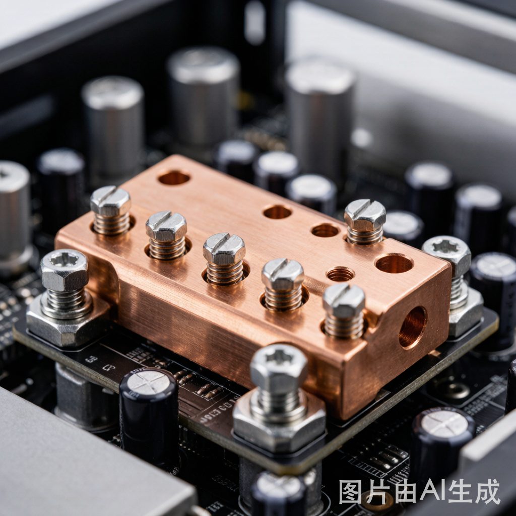
Mechanical Forming and Attachment
Busbar shapes are typically produced by CNC bending, stamping, or progressive die forming. Common geometries include:
- Flat strip: Simple straight conductors for PCB edge-to-edge co
ection
- Bent L-shape or U-shape: Vertical offsets to bridge components at different elevations
- Laminated copper: Multiple thin copper sheets insulated by dielectric film, providing superior AC performance at high frequencies (reduced skin effect losses) for high-frequency power converter applications
- Busbar with integrated heat sink: Thicker copper sections or bonded aluminum heat sinks for thermal management of high-I²R loss regions
Mechanical attachment to PCBs uses several methods: through-hole soldering (most robust), SMT soldering (lowest cost, requires precise coplanarity), bolted lugs (high current, field-serviceable), or compression contacts (no solder, modular assembly). The choice depends on current level, vibration environment, and assembly process requirements.
Thermal Management
High-current busbars generate significant I²R heat, which must be dissipated to maintain operating temperature within safe limits (typically <105°C for tin-plated copper, <150°C for nickel-plated). Strategies include:
- Increased cross-section: Direct reduction in I²R loss; most effective approach
- Forced air cooling: Busbars in enclosed enclosures benefit from forced airflow across their surface; typical convection coefficient 50–200 W/m²·K
- Bonded heat sinks: Aluminum or copper heat sinks bonded via thermal interface material (TIM) absorb and distribute heat
- Direct bonding to PCB copper: Busbar soldered to large PCB copper areas conducts heat directly into the board, leveraging the PCB as a heat spreader
For EV and renewable applications, laminated busbars with integral thermal management (water-cooled or heat-sink integrated) are increasingly common in 100+ kW power converter designs.
SMT Integration: Process and Reliability Considerations
Integrating copper busbars into SMT-assembled products requires careful process pla
ing:
- Coplanarity: Busbar pad flatness must be <0.1 mm across all attachment points to ensure uniform solder joint formation
- Solder joint inspection: AOI is challenging for tall busbar joints; X-ray inspection verifies through-hole solder fill; cross-sectioning may be required for qualification
- Reflow profile: Busbars have high thermal mass; extended preheat zones and longer soak times (90–120 seconds at 150–200°C) ensure uniform heating and prevent thermal shock
- Mechanical stress: Busbar CTE mismatch with PCB (copper 17 ppm/°C vs. FR-4 z-axis 60 ppm/°C) generates solder joint stress in thermal cycling; mechanical strain relief (flexible sections, S-bends) reduces fatigue
- Selective soldering: For through-hole busbar attachment, selective wave soldering provides localized heating that protects nearby SMT components
EMI and EMC Considerations
High-current busbars are potential EMI sources due to fast dI/dt switching in power converters. Best practices include:
- Minimize loop area: The high-current loop (DC bus to switching device to load and back) should be as physically small as possible to reduce radiated EMI
- Laminated busbars: For switching frequencies above 20 kHz, laminated busbars with tightly coupled positive and negative conductors dramatically reduce loop inductance and radiated EMI
- Snubber capacitors: Localized film or ceramic capacitors across the DC bus reduce high-frequency voltage transients
- Shielding: In EMI-sensitive applications, busbars can be enclosed in grounded metal shrouds or shielded cables
Conclusion
Copper busbars remain the most efficient, reliable, and cost-effective solution for high-current power distribution in modern electronics. From EV powertrains to data center power supplies, the combination of high conductivity, mechanical robustness, and SMT-compatible assembly makes busbars indispensable in power electronics. Successful busbar design requires careful balance of current capacity, voltage drop, thermal management, and electromagnetic compatibility—with material and plating choices tailored to the specific demands of each application environment.