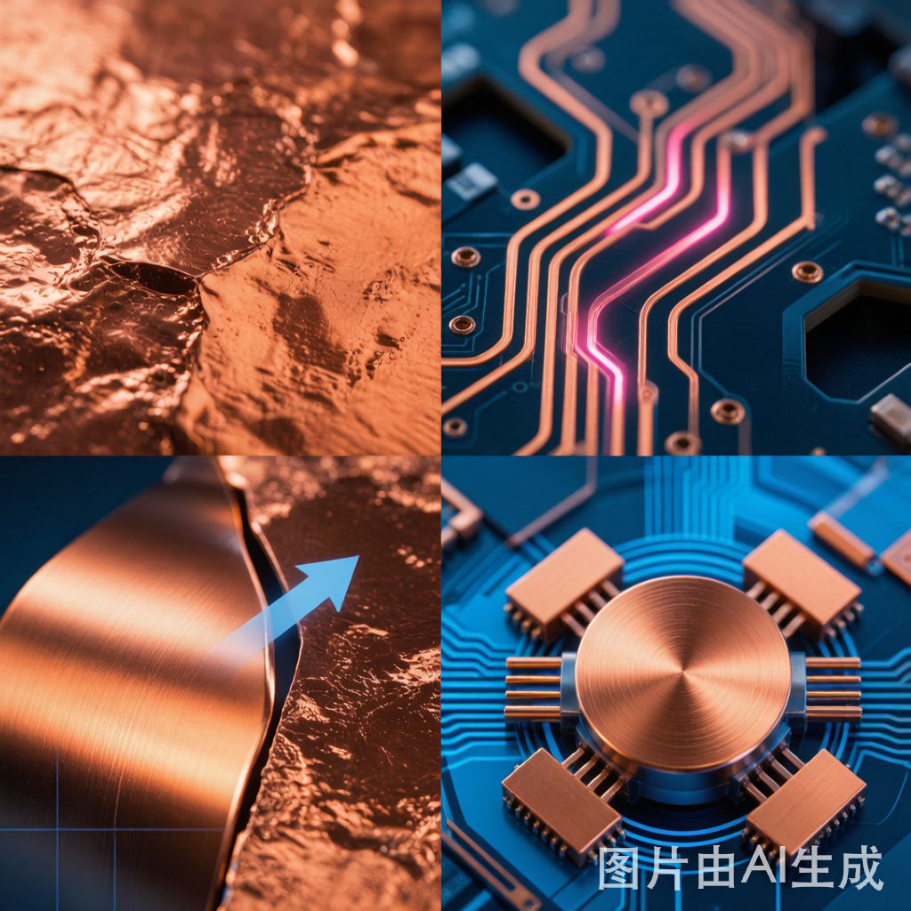
Why Copper Roughness Matters at High Frequencies
In low-speed digital circuits, the surface roughness of copper foil on a PCB is of little consequence — current flows through the full cross-section of the trace, and the additional path length caused by roughness is negligible. However, as signal frequencies push into the GHz range, the skin effect concentrates current flow into an increasingly thin layer at the copper surface. When the skin depth becomes comparable to the surface roughness profile, the effective resistance of the trace increases dramatically, leading to higher insertion loss, signal attenuation, and degraded eye diagrams.
At 10 GHz, the skin depth in copper is approximately 0.66 μm — thi
er than the typical surface roughness (Rz) of standard electrodeposited (ED) copper foil, which ranges from 5-10 μm. At these frequencies, the current is forced to follow the contours of the rough surface, effectively traveling a longer path than the nominal trace length. This phenomenon, known as the hammerstad roughness correction, can increase conductor loss by 10-40% depending on the foil type and frequency.
Understanding Copper Foil Profile Types
PCB copper foils are categorized by their manufacturing process and surface profile:
Electrodeposited (ED) Copper
ED copper is the most common and economical foil type, produced by electroplating copper onto a rotating drum. The drum side is relatively smooth (the “shiny” side), while the solution side (the “matte” side) has a characteristic nodular or dendritic structure that provides adhesion to the prepreg. The matte-side roughness (Rz) can range from 5-12 μm depending on the foil grade.
- Standard ED foil (STD): Rz ≈ 8-12 μm, highest roughness, adequate for frequencies below 1 GHz
- Reverse-treated foil (RTF): Rz ≈ 4-8 μm, drum side bonded to prepreg, moderately improved high-frequency performance
- Low-profile foil (LP): Rz ≈ 3-5 μm, reduced nodular treatment, suitable for 1-10 GHz designs
- Very-low-profile foil (VLP): Rz ≈ 1.5-3 μm, minimal roughness, optimized for 10+ GHz and 5G mmWave applications
Rolled A
ealed (RA) Copper
RA copper is produced by mechanically rolling and a
ealing copper ingots into thin foils. The rolling process creates an extremely smooth surface (Rz < 1 μm on both sides), making RA copper the preferred choice for flexible circuits and the highest-frequency rigid PCB applications. However, RA copper is more expensive and provides less mechanical adhesion to prepreg, typically requiring a silane coupling agent treatment.
Quantifying Roughness-Induced Loss
The impact of copper roughness on insertion loss is modeled using correction factors applied to the smooth-conductor attenuation constant. The most widely used model is the Hammerstad-Jensen correction:
Krough = 1 + (2/π) · arctan(1.4 · (Rq/δ)2)
where Rq is the RMS surface roughness and δ is the skin depth. More sophisticated models, such as the Huray “snowball” model, treat the surface as a distribution of spherical nodules and provide better agreement with measured data above 20 GHz.
Practical insertion loss comparison for a 50 Ω microstrip on Megtron 6 laminate (Dk=3.7, Df=0.002) at 10 GHz:
- Standard ED: ~0.85 dB/inch — unacceptable for most high-speed serial links
- RTF: ~0.70 dB/inch — marginal for 10 Gbps NRZ, adequate for 5 Gbps
- VLP: ~0.55 dB/inch — acceptable for 28 Gbps NRZ up to ~12 inches
- RA/HVLP: ~0.45 dB/inch — suitable for 56 Gbps PAM4 and 5G mmWave
Design Strategies for Roughness Mitigation
When designing high-speed PCBs, engineers should consider the following strategies:
- Specify VLP or HVLP copper on all high-speed signal layers — the cost premium is modest compared to the signal integrity benefit
- Use wider traces for critical signals — wider traces have lower current density and are proportionally less affected by roughness
- Route critical signals on i
er layers with RA copper
— stripline configurations with smooth copper on both reference planes minimize insertion loss - Work with your fabricator to characterize roughness — request insertion loss test coupons (SET2DIL or similar) for each lot
- Account for roughness in simulation — use the Huray model rather than Hammerstad for designs above 20 GHz
As data rates continue their relentless climb — with 112 Gbps PAM4 and 224 Gbps on the horizon — copper foil roughness will remain a critical parameter in the PCB designer’s toolkit. A few microns of roughness can mean the difference between an open eye diagram and a closed one.


