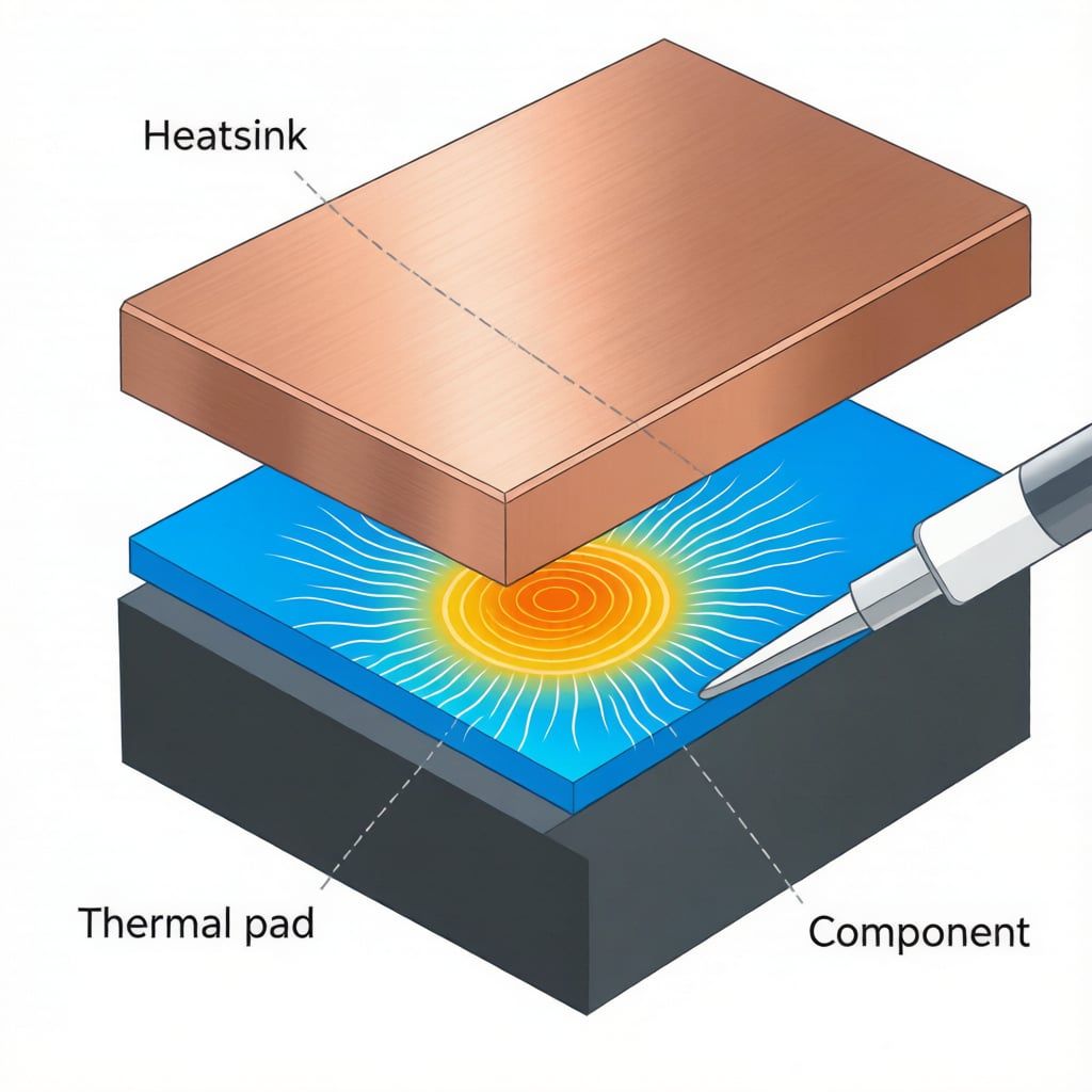
Why Gap Fillers Are Essential in Heatsink Assemblies
In an ideal world, the mating surfaces of a copper heatsink and a power semiconductor package would be perfectly flat and smooth, allowing near-perfect thermal contact. In reality, surface roughness, component height tolerances, and PCB warpage create air gaps that dramatically increase the thermal resistance between the heat source and the cooling solution.
Thermal gap filler pads are compliant, thermally conductive materials that fill these air gaps, displacing the low-conductivity air (~0.026 W/m·K) with materials that conduct heat 100 to 1000 times more effectively. For SMT power electronics — where MOSFETs, IGBTs, GaN devices, and power modules dissipate tens or hundreds of watts — proper gap filler selection is critical to meeting thermal design targets.
Key Material Properties and How to Evaluate Them
Thermal Conductivity (k)
Thermal conductivity is the primary specification engineers look at, typically ranging from 1 W/m·K for basic silicone pads to 20+ W/m·K for advanced graphite or boron nitride-filled materials. However, thermal conductivity numbers in datasheets can be misleading because there is no universally adopted standard for measurement.
Key caveats when comparing thermal conductivity values:
- ASTM D5470 (steady-state) and laser flash (transient) methods yield different results for the same material
- Some manufacturers report bulk conductivity while others report effective (in-application) conductivity
- Pressure, temperature, and thickness all affect measured values
- Always request the test method when comparing materials from different suppliers
Hardness and Compressibility
The Shore OO hardness scale is commonly used for gap fillers, with values ranging from 10 (very soft gel-like) to 80 (firm rubber). A softer pad compresses more easily but may not provide sufficient contact pressure, while a harder pad may require excessive mounting force that stresses the PCB.
Compression-deflection curves (stress vs. strain) are more informative than single-point hardness values. The ideal operating point is typically 20-40% compression, where thermal resistance is minimized without excessive mechanical stress on components or solder joints.
Compression Set
Compression set measures how much of the initial compression is permanently lost after the material is held under compression at elevated temperature and then released. A high compression set means the pad loses contact force over time, degrading thermal performance. For long-lifetime applications (automotive, industrial, base station), look for materials with compression set below 10% after 24 hours at rated temperature.
Surface Wetting and Thermal Contact Resistance
The thermal resistance of a gap filler assembly is not determined by bulk conductivity alone. The thermal contact resistance at the interface between the pad and the mating surfaces often dominates the total resistance. Soft, conformable pads with a naturally tacky surface achieve lower contact resistance because they deform to fill microscopic surface irregularities.
Strategies to minimize contact resistance:
- Specify the pad slightly thicker than the nominal gap (e.g., 1.0 mm pad for a 0.8 mm gap) to ensure adequate compression
- Clean mating surfaces with isopropyl alcohol before assembly
- Use pads with inherent surface tack rather than applying additional thermal grease
- For critical applications, consider phase-change materials that melt and flow under operating temperatures to fill microscopic voids
Material Types and Selection Guide
| Material Type | k (W/m·K) | Hardness | Best Application |
|---|---|---|---|
| Silicone elastomer (Al₂O₃-filled) | 1-3 | Shore OO 30-60 | General-purpose, low-cost |
| Silicone (BN-filled) | 3-8 | Shore OO 25-50 | Medium power, good compliance |
| Silicone (ceramic-filled) | 8-15 | Shore OO 40-70 | High power, moderate compliance |
| Non-silicone (acrylic/urethane) | 2-6 | Shore OO 30-50 | Silicone-sensitive (optical, medical) |
| Graphite pad | 10-20+ | Firm (compressible) | Highest conductivity, large gaps |
| Phase-change material | 3-8 | Solid → liquid at Tm | Cyclic loads, best surface wetting |
Validation and Reliability Testing
Before committing to production, gap filler assemblies should be validated through:
- Steady-state thermal testing: Measure junction temperature (Tj) rise at rated power with actual assembly configuration
- Thermal cycling: 500-1000 cycles, -40°C to +125°C per JEDEC JESD22-A104 to verify no pad extrusion or loss of contact
- High-temperature storage: 1000 hours at rated maximum temperature to quantify compression set and thermal degradation
- Vibration testing: Per application requirements (e.g., automotive: ISO 16750-3) to verify mechanical stability
A well-selected thermal gap filler pad, properly compressed between a copper heatsink and the heat-generating component, can reduce junction temperature by 10-20°C compared to an unoptimized assembly — often the difference between passing and failing thermal qualification.


