The Evolution from Solder Bumps to Copper Pillars
Flip-chip packaging has been the dominant interco
ect technology for high-performance semiconductors for decades. Traditionally, flip-chip co
ections were made using solder bumps — typically lead-tin or lead-free SAC (Sn-Ag-Cu) alloys deposited on the die pads. While solder bumps served the industry well, they face fundamental limitations as bump pitch decreases below 150 μm.
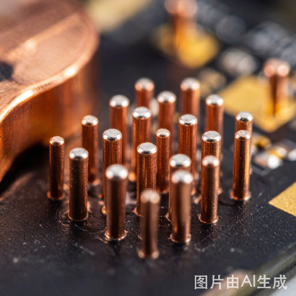
Copper pillar bump technology addresses these limitations directly. A copper pillar is a tall, narrow column of electroplated copper — typically 30-80 μm in height and 20-50 μm in diameter — capped with a small volume of solder (usually SnAg). The copper pillar provides superior electrical performance, finer pitch capability, and better thermal management compared to conventional solder bumps.
Copper Pillar Process Flow
The manufacturing process for copper pillar bumps involves several sequential steps on the wafer:
- Under-Bump Metallization (UBM): A thin adhesion/diffusion barrier layer (typically Ti/Cu or TiW/Cu) is sputtered onto the aluminum pad to ensure reliable electrical contact
- Photolithography: A thick photoresist (30-100 μm) is patterned to define the pillar locations
- Copper electroplating: High-purity copper is electroplated into the mold openings to form the pillar body
- Solder cap plating: A thin layer of SnAg or pure Sn solder is plated on top of the copper pillar
- Resist stripping and UBM etching: The photoresist is removed and the UBM seed layer is etched away
- Reflow: The solder cap is reflowed to form a smooth dome shape ready for bonding
Key Advantages Over Traditional Solder Bumps
Copper pillar technology offers several decisive advantages:
- Fine pitch capability: Copper pillars can achieve bump pitches as low as 40 μm (vs. 130-150 μm minimum for solder bumps), enabling higher I/O density
- Superior electrical performance: Copper’s lower resistivity (1.7 μΩ·cm vs. 12-15 μΩ·cm for solder) reduces IR drop and improves power delivery
- Better electromigration resistance: Copper’s higher melting point and stronger atomic bonding provide 10-100x better electromigration lifetime
- Improved thermal conductivity: Copper (400 W/m·K) conducts heat 5-8 times better than solder alloys (50-60 W/m·K)
- Controlled standoff height: The rigid copper pillar maintains precise die-to-substrate gap, eliminating solder collapse variability
Underfill Considerations for Copper Pillar Assemblies
After flip-chip bonding, the gap between the die and substrate must be filled with an underfill encapsulant to absorb CTE mismatch stress and protect the interco
ects from moisture and contamination. Copper pillar assemblies present specific underfill challenges:
- The smaller gap height (as low as 20-30 μm) requires lower-viscosity underfill materials with finer filler particles
- Flow time is proportional to the square of gap height — underfill must be carefully engineered for capillary flow in narrow gaps
- Molded underfill (MUF) or non-conductive paste (NCP) may be preferred for ultra-fine-pitch applications where capillary underfill is impractical
Applications and Industry Adoption
Copper pillar bump technology is now widely deployed across the semiconductor industry:
- Mobile processors and SoCs: Apple A-series, Qualcomm Snapdragon, and Samsung Exynos processors use copper pillars for high-density interco
ect
- High-bandwidth memory (HBM): 3D-stacked DRAM uses copper pillar microbumps with pitches below 55 μm
- FPGAs and ASICs: Xilinx/AMD and Intel use copper pillars for their advanced packaging platforms
- CMOS image sensors: Copper pillars enable thi
er camera modules with higher resolution sensors
As the semiconductor industry pushes toward chiplet architectures and heterogeneous integration, copper pillar technology will continue to play a central role in co
ecting diverse dies within advanced packages.


