Why CTE Mismatch Threatens BGA Solder Joint Integrity
Ball Grid Array (BGA) packages are the backbone of modern SMT electronics, from smartphone processors to server-grade FPGAs. Yet every BGA sits atop a copper-clad laminate (CCL) substrate with a fundamentally different coefficient of thermal expansion (CTE). As the assembly heats and cools — during operation, rework, or environmental cycling — this CTE mismatch generates shear forces that fatigue the solder joints, eventually causing cracks, opens, and catastrophic field failures.
The problem is intensifying as package sizes grow (76mm+ FPGAs are now common), power dissipation increases, and operating temperature ranges widen — especially for automotive and industrial electronics operating from -40°C to +125°C. A 50mm BGA on standard FR-4 CCL experiencing a 100°C temperature swing accumulates enough differential strain to initiate solder joint cracking within 500-2,000 thermal cycles, depending on joint geometry and solder alloy.
Understanding the CTE mismatch mechanism and designing to mitigate it is essential for any SMT assembly that must survive in the field for 5, 10, or 15 years. This article examines the physics, failure modes, and practical countermeasures for CTE-mismatch-induced BGA solder joint fatigue.
Understanding CTE Values in SMT Assemblies
CTE — measured in parts per million per degree Celsius (ppm/°C) — quantifies how much a material expands or contracts with temperature change. In a BGA-on-CCL assembly, three material CTEs interact:
FR-4 CCL (in-plane X/Y): 12-18 ppm/°C, depending on glass weave style, resin content, and copper coverage. High-Tg FR-4 (multifunctional epoxy) typically shows 14-16 ppm/°C. The copper layers constrain in-plane expansion somewhat, but the dominant CTE is set by the glass-epoxy composite.
FR-4 CCL (out-of-plane Z): 50-70 ppm/°C, dramatically higher than in-plane because the glass fabric provides no constraint through the thickness. Z-axis expansion is relevant for plated through-hole reliability but less directly for BGA solder joints.
BGA Package (organic substrate, in-plane): 12-17 ppm/°C for PBGA (plastic BGA on BT laminate), which is reasonably close to FR-4. The effective CTE depends on the die-to-substrate area ratio and the substrate construction.
BGA Package (ceramic): 6-8 ppm/°C for alumina (CBGA/CCGA). The large CTE gap between ceramic BGAs and FR-4 (6-8 vs 14-16 ppm/°C) makes ceramic packages dramatically more susceptible to solder joint fatigue. This is the classic high-risk CTE mismatch scenario.
Solder Joint (SAC305): 22-25 ppm/°C. The solder itself has a CTE higher than either the package or the PCB, adding to the strain gradient across the joint height.
Effective DNP (Distance from Neutral Point): The critical parameter for solder joint strain. The neutral point is typically the center of the BGA. Solder joints at the corners — farthest from the neutral point — experience the maximum differential displacement. A 50mm BGA has corner joints at approximately 25mm DNP; a 35mm BGA at 17.5mm DNP. Strain is proportional to DNP, so larger packages are inherently more vulnerable.
Failure Mechanisms: From Thermal Cycling to Crack Initiation
Solder joint fatigue follows a well-characterized sequence driven by CTE-mismatch-induced shear strain:
Cyclic Shear Strain Accumulation: Each thermal cycle imposes a shear strain (γ) on the solder joint proportional to: γ = (Δα × ΔT × DNP) / h, where Δα is the CTE difference, ΔT is the temperature swing, DNP is the distance from neutral point, and h is the joint height. For a ceramic BGA on FR-4: γ ≈ (10 ppm/°C × 100°C × 25mm) / 0.5mm = 0.05 (5% shear strain per cycle).
Crack Initiation: Repeated cycling causes microstructural coarsening of the solder intermetallic compound (IMC) layer, creating stress concentration sites. Cracks typically initiate at the solder-to-copper pad interface (the IMC layer) on the component side, where the strain is highest due to the constraint of the copper pad.
Crack Propagation: Once initiated, cracks propagate across the solder joint cross-section at a rate governed by the cyclic strain range and solder properties. SAC305 (Sn-Ag-Cu) solder exhibits slower crack growth than legacy Sn-Pb solder for low strain ranges, but faster growth at high strain ranges — a critical distinction for large ceramic BGAs.
Electrical Failure: The joint fails when the crack propagates through enough of the cross-section to cause intermittent contact (detected as bit errors or functional failures under vibration) or complete open circuit. Typical failure occurs when the crack covers 50-70% of the joint area.
Material Selection Strategies for CTE Mitigation
The most effective approach to CTE mismatch is reducing the CTE differential through material selection:
High-Tg, Low-CTE FR-4: Multifunctional and polyimide-based CCL materials achieve CTE values of 10-13 ppm/°C in-plane, reducing the gap with ceramic packages from ~10 ppm/°C to ~4-5 ppm/°C. Materials like Isola FR408HR (CTE ~12 ppm/°C), Megtron 6 (CTE ~11 ppm/°C), and Rogers 4350B (CTE ~10-11 ppm/°C) provide meaningful CTE reduction at moderate cost premium (1.5-3× standard FR-4).
Copper-Invar-Copper (CIC) Constrained Cores: Embedding a low-CTE Invar (Fe-36Ni, CTE ~1.2 ppm/°C) core clad with copper into the PCB stackup constrains the overall in-plane CTE to 5-8 ppm/°C, closely matching ceramic packages. CIC cores add cost and weight but provide the most dramatic CTE reduction possible in a standard PCB construction.
Aramid Fiber Reinforcement: Thermount or similar aramid-fiber reinforced CCL achieves in-plane CTE of 6-9 ppm/°C, closely matching ceramic packages. Aramid CCL is lighter than CIC solutions but has lower thermal conductivity and higher moisture absorption, requiring careful process control.
Package-Level Solutions: Selecting PBGA packages (organic substrate, CTE ~14-16 ppm/°C) instead of ceramic packages (CTE ~6-8 ppm/°C) eliminates the most severe CTE mismatch at the source. For high-performance designs that require ceramic packages, consider column grid array (CCGA) packages with compliant solder columns that absorb the differential strain.
Underfill and Mechanical Reinforcement
When material selection alone ca
ot adequately reduce the CTE mismatch, mechanical reinforcement strategies extend solder joint fatigue life:
Capillary Underfill: Epoxy-based filler dispensed along one edge of the BGA, drawn by capillary action to fill the gap between the package bottom and PCB surface. Underfill bonds the package to the PCB, distributing the CTE-induced shear strain across the entire underfill area rather than concentrating it in the solder joints. Typical fatigue life improvement: 5-10× for ceramic BGAs, 2-4× for organic BGAs.
No-Flow Underfill: Applied before BGA placement, the underfill material also serves as the flux for soldering. The BGA is placed into the wet underfill, and reflow soldering and underfill cure occur simultaneously. Simpler process but less control over fillet quality and void content.
Corner/Edge Bonding: A compromise between full underfill and no reinforcement. Epoxy is applied only to the corner or edge solder joints — the highest-strain locations — providing targeted reinforcement with lower material cost and easier rework than full underfill. Typical improvement: 2-3× fatigue life at the critical corner joints.
Edge Staking: Similar to corner bonding but uses a more flexible adhesive (typically silicone or urethane) that absorbs strain rather than rigidly bonding the package. Less effective than rigid underfill for extreme CTE mismatches but preserves reworkability.
Design Guidelines for Thermally Robust BGA Assemblies
Practical design rules that minimize CTE-mismatch risk:
Package Size Limits: For standard FR-4 (CTE ~14-16 ppm/°C) without underfill, limit organic BGA package size to 45mm maximum for 0-100°C cycling and 35mm for -40°C to +125°C cycling. For ceramic packages, limit to 25mm without underfill and 40mm with underfill.
Solder Mask Defined (SMD) vs Non-Solder Mask Defined (NSMD) Pads: NSMD copper pads (where solder mask opens larger than the copper pad) provide better solder joint reliability because the solder wets the pad sidewalls, increasing the effective joint cross-section. SMD pads concentrate stress at the pad edge. Use NSMD pads for BGA footprints whenever possible.
Joint Height Optimization: Taller solder joints reduce shear strain (strain is inversely proportional to joint height). For large BGAs, consider using 0.5mm or 0.6mm solder spheres instead of the standard 0.3mm, and use thicker copper pads (2 oz) on the PCB side to increase the effective standoff height after reflow.
Thermal Via Management: Excessive thermal vias in the BGA land area can locally reduce the PCB’s effective CTE (copper has lower CTE than FR-4), potentially increasing the CTE mismatch with the package. Balance thermal via count against the CTE impact. Typically, limit thermal via density to one via per BGA pad maximum.
Component Placement: Place large BGAs away from board edges and mounting points, where mechanical flexure from board bending adds to the CTE-induced strain. Central board locations experience the least mechanical flexure.
Testing and Qualification
Validating BGA solder joint reliability for CTE-mismatch-sensitive assemblies requires accelerated thermal cycling tests:
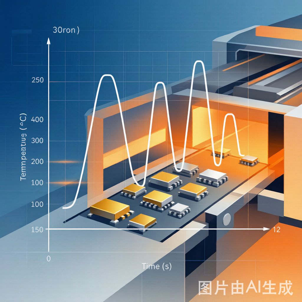
IPC-9701 Thermal Cycling: The industry standard for solder joint reliability qualification. Test conditions: 0°C to +100°C (TC1), -25°C to +125°C (TC2), or -40°C to +125°C (TC3), with 10-15 minute dwell times at temperature extremes and ramp rates of 10-15°C/minute. Monitor daisy-chain resistance for intermittent opens (20% resistance increase = failure). Report characteristic life (63.2% failure rate) in cycles.
Acceptable Life Targets: For commercial electronics, 1,000-3,000 cycles to characteristic life is typically acceptable (corresponding to 5-10 years field life under normal operating conditions). For automotive and industrial, target 3,000-6,000 cycles. For aerospace and military, 6,000+ cycles may be required.
Conclusion
CTE mismatch between copper-clad laminate and BGA packages is a fundamental physics challenge that ca
ot be eliminated — only managed. The key strategies, in order of effectiveness, are: (1) selecting package and PCB materials with closely matched CTEs, (2) using underfill to distribute strain away from solder joints, and (3) optimizing joint geometry and pad design to maximize fatigue resistance.
For SMT designers working with large BGAs in thermally demanding applications, the CTE mismatch calculation should be a first-order design parameter, not an afterthought. A proactive approach — matching CTEs at the material selection phase — costs far less than field failures and warranty claims. When CTE matching is insufficient, underfill provides a proven, reliable second line of defense that has become standard practice in automotive, aerospace, and high-reliability electronics manufacturing.


