Introduction to Solder Paste Stencils in SMT Assembly
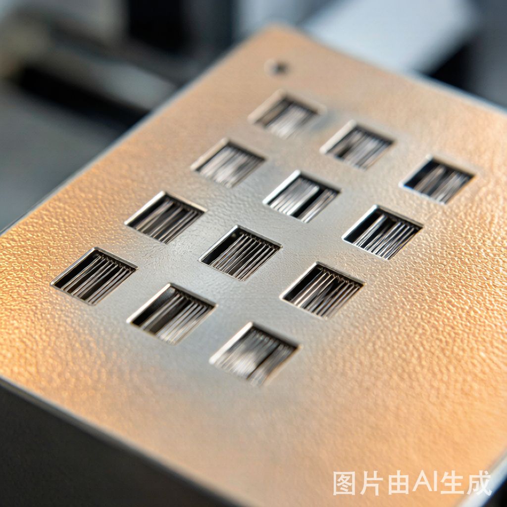
Solder paste stencils are one of the most critical tools in surface mount technology (SMT) assembly. These thin metal foils with laser-cut apertures define exactly how much solder paste deposits onto each copper pad on a printed circuit board (PCB). The quality of your stencil design directly impacts solder joint reliability, defect rates, and overall manufacturing yield.
For electronics manufacturers in Southeast Asia and beyond, stencil printing accounts for 60-70% of all SMT defects according to industry studies. Understanding the relationship between stencil aperture geometry, copper pad design, and solder paste rheology is essential for achieving consistent, high-quality results.
In this guide, we explore the fundamental principles of solder paste stencil design specifically for copper PCB pads, covering aperture ratios, foil thickness selection, and practical optimization techniques that SMT engineers can apply immediately.
Understanding Stencil Aperture Geometry and Area Ratio
The aperture ratio is the single most important parameter in stencil design. For rectangular apertures, the area ratio is calculated as the opening area divided by the wall area:
Area Ratio = (L × W) / [2 × (L + W) × T]
Where L = length, W = width, and T = stencil thickness.
Industry standards recommend a minimum area ratio of 0.66 for standard solder paste printing. For fine-pitch components (0.5mm pitch and below), a ratio of 0.50 or higher is achievable with electroformed stencils and modern solder pastes with fine powder particles (Type 4 or Type 5).
When designing for copper pads, consider the pad finish. OSP (Organic Solderability Preservative) and ENIG (Electroless Nickel Immersion Gold) surfaces behave differently during paste release. Gold pads tend to have slightly better paste release characteristics due to their smoother surface, while OSP-coated copper may require slightly larger apertures to compensate for paste adhesion.
Choosing the Right Stencil Foil Thickness
Stencil thickness typically ranges from 0.08mm to 0.15mm (3 to 6 mils). The correct thickness depends on your component mix and the smallest paste deposit required:
0.10mm (4 mil): Ideal for fine-pitch QFP, BGA with 0.5mm pitch, and 0201 passives. Most common in consumer electronics.
0.12mm (5 mil): Good general-purpose thickness for mixed-technology boards with components ranging from 0402 to larger ICs.
0.15mm (6 mil): Suitable for power electronics, co
ectors, and boards requiring larger solder volumes for through-hole components in a mixed SMT/THT process.
For step stencils, which feature different thicknesses in different board regions, a common approach is 0.10mm in fine-pitch areas and 0.15mm in power component zones. This dual-thickness approach allows optimal paste volume for both fine-pitch ICs and power devices on the same board.
Aperture Design Rules for Common Component Types
Different SMT components require different stencil aperture strategies:
QFP and Fine-Pitch ICs: Reduce aperture width by 10-15% compared to pad width to prevent bridging. Maintain 1:1 length ratio. For 0.5mm pitch QFP, typical aperture dimensions are 0.20mm × 1.0mm on a 0.10mm stencil.
BGA (Ball Grid Array): Aperture size typically 85-90% of the solder ball diameter for standard BGA. For 0.4mm pitch micro-BGA, use Type 5 solder paste and electroformed stencils for reliable release.
0402/0201 Passives: Keep apertures at 1:1 with pad dimensions or slightly undersized (5% reduction on each side). Ensure the area ratio stays above 0.50 for 0201 components on 0.10mm stencils.
Power Components (D2PAK, DPAK): These require significantly more solder paste. Use expanded apertures or step-down regions with thicker stencil sections. A 50-100% increase in aperture area compared to the pad is common practice.
Optimizing Paste Release and Print Quality
Achieving consistent paste release from the stencil is a combination of design, materials, and process parameters:
Foil Material Selection: Stainless steel is the standard choice for most applications. Electroformed nickel stencils offer superior aperture smoothness for ultra-fine-pitch printing. Polyimide stencils with laser-cut apertures are used for prototyping.
Nano-Coating Benefits: Applying a hydrophobic nano-coating to the stencil underside reduces paste adhesion to the stencil walls, improving transfer efficiency by 5-15%. This is particularly valuable for Type 4 and Type 5 solder pastes used in fine-pitch applications.
Print Parameters: Squeegee speed (25-75mm/s), squeegee pressure (0.5-1.0 kg/cm), and separation speed all affect print quality. Faster separation speeds (0.5-1.0 mm/s) help paste release from fine apertures but may cause smearing on larger deposits.
Inspection and Feedback: Automated optical inspection (AOI) of printed paste deposits should be integrated into every SMT line. SPI (Solder Paste Inspection) systems measure deposit volume, height, and area in real-time.
Common Stencil-Related Defects and Solutions
Understanding and preventing common printing defects is key to maintaining high SMT yield:
Solder Bridging: Caused by excessive paste volume or apertures that are too wide. Reduce aperture width by 10-20%, verify stencil alignment, and check squeegee blade condition.
Insufficient Paste Volume: Results from undersized apertures, poor paste release, or clogged stencil openings. Clean stencils regularly, verify paste properties, and consider nano-coating.
Tombstoning: Uneven paste volumes across a component’s two terminals cause asymmetric wetting forces during reflow. Ensure symmetrical aperture design and consistent print quality.
Scooping: Occurs when the squeegee removes paste from larger apertures. Use step stencils for boards with mixed component sizes, or reduce squeegee pressure.
Conclusion
Effective solder paste stencil design is a blend of engineering fundamentals and practical experience. For copper PCB pads, paying close attention to area ratios, foil thickness selection, and aperture sizing for each component type will dramatically improve your SMT printing quality and reduce defect rates.
As component pitches continue to shrink and board complexity increases, investing in quality stencil design and modern stencil technologies — such as electroformed foils, nano-coatings, and step stencils — becomes increasingly important for competitive electronics manufacturing.
Whether you are setting up a new SMT line or optimizing an existing process, the principles outlined in this guide provide a solid foundation for achieving excellent solder paste printing results on copper PCB pads.


