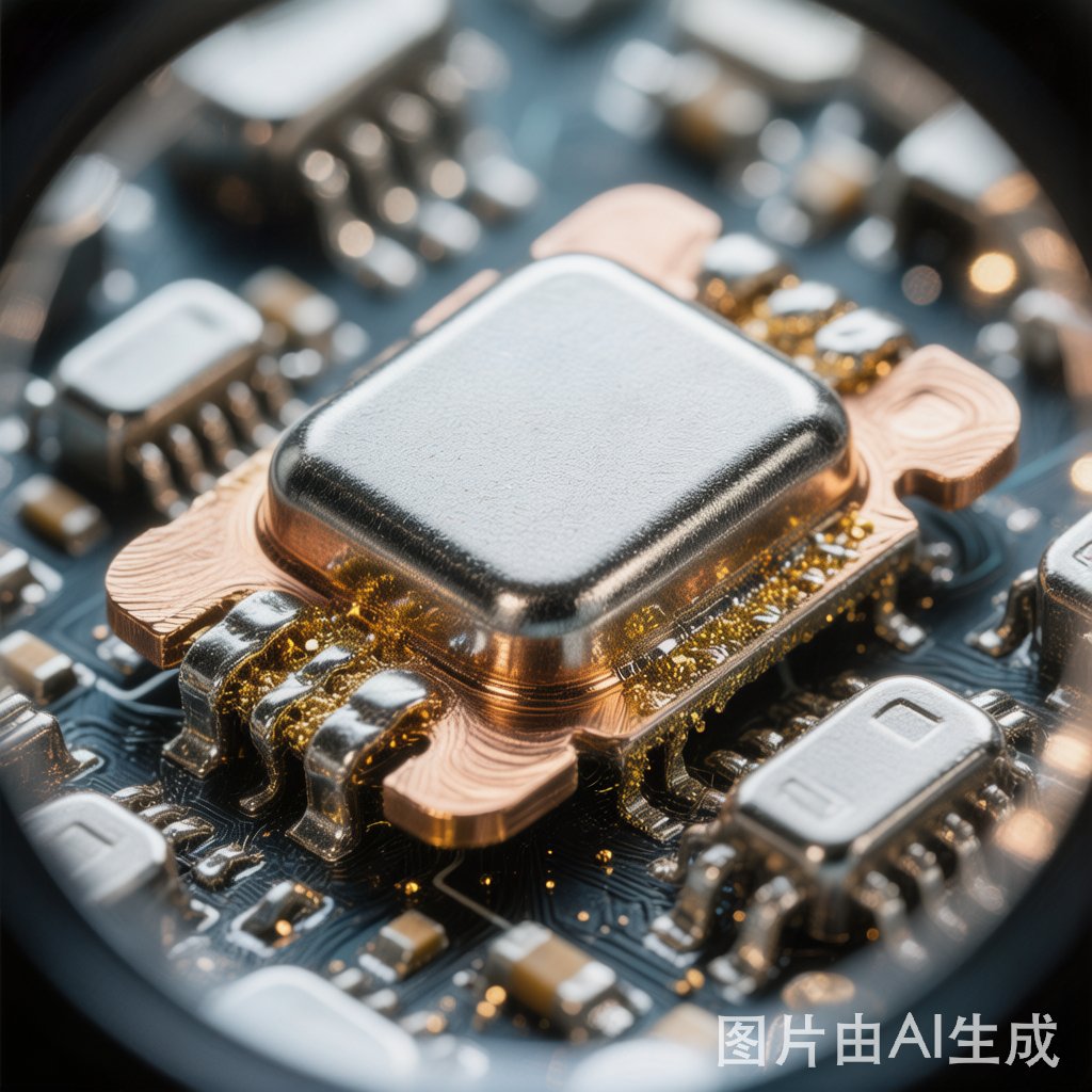
Introduction
Nickel plating on copper strips serves dual purposes in electronics manufacturing: it provides a protective barrier against copper oxidation and creates a solderable surface for SMT assembly. However, nickel’s soldering behavior differs substantially from bare copper or gold-plated surfaces, and understanding these differences is essential for achieving reliable, void-free solder joints in high-volume production.
Why Nickel-Plate Copper Strips?
Copper strip components in SMT applications — EMI shield frames, co
ector leads, and bus bar tabs — frequently receive nickel plating for several compelling reasons:
- Oxidation resistance: Copper oxidizes rapidly in ambient conditions, forming a non-solderable surface within hours. Nickel’s oxide layer grows much more slowly and remains thin enough for flux activation
- Diffusion barrier: Nickel prevents copper from diffusing into the solder joint during reflow, maintaining the joint’s mechanical integrity over thermal cycling
- Solderability shelf life: Nickel-plated surfaces maintain solderability for 12+ months under proper storage, compared to days for bare copper
- Wear resistance: For co
ector applications, nickel under gold provides a hard sub-layer that prevents gold wear-through to the copper base
The Chemistry of Soldering to Nickel
When Sn-based solder alloys (SAC305, Sn63Pb37) wet a nickel surface during reflow, intermetallic compound (IMC) formation is fundamentally different from copper soldering:
- Cu-Sn IMC (copper-to-solder): Cu₆Sn₅ and Cu₃Sn form rapidly, growing 2–4 μm during a typical reflow cycle
- Ni-Sn IMC (nickel-to-solder): Ni₃Sn₄ forms more slowly, typically reaching only 1–2 μm during reflow
This slower IMC growth on nickel is generally beneficial — thi
er IMC layers are less brittle — but it also means that nickel surfaces are less forgiving of contamination or insufficient flux activation.
Critical Parameters for Successful Nickel Soldering
1. Plating Thickness Optimization
Nickel plating thickness has a sweet spot for soldering:
- Too thin (<1 μm): Porosity allows copper diffusion through pinholes, negating the barrier benefit
- Optimal (2–5 μm): Dense, non-porous surface with good solderability
- Too thick (>10 μm): Internal stress in the nickel layer can cause cracking during forming or thermal cycling. Also increases cost without proportional benefit
2. Surface Preparation and Cleanliness
Nickel surfaces are sensitive to organic contamination. Even fingerprint residue can cause dewetting. Best practices include:
- Vacuum-sealed packaging with desiccant for storage
- Plasma cleaning immediately before solder paste printing for critical applications
- Avoiding handling with bare hands — use gloves or vacuum pick-up tools
3. Flux Selection Matters
Nickel requires more aggressive flux activation than copper or gold. For reliable soldering:
- Water-washable fluxes with activation temperature above 150°C provide the best wetting on nickel surfaces
- No-clean fluxes should be selected carefully — ROL1 (rosin, mildly activated) may not provide adequate oxide removal on aged nickel surfaces
- Avoid halide-free fluxes for nickel unless specifically validated, as nickel oxides are more tenacious than copper oxides
Common Soldering Defects and Root Causes
| Defect | Likely Cause | Solution |
|---|---|---|
| Dewetting / non-wetting | Surface contamination or passivation | Plasma clean; switch to higher-activity flux |
| Solder balling | Insufficient flux activation; too-rapid preheat | Extend soak zone 150–180°C by 10–20 seconds |
| Voids in joint | Outgassing from plating bath residues | Bake components at 125°C for 2–4 hours before assembly |
Reflow Profile Adjustments for Nickel-Plated Parts
Compared to standard copper pad soldering, nickel-plated components benefit from these profile tweaks:
- Extended soak: 90–120 seconds above 150°C gives flux activators adequate time to clean the nickel surface
- Higher peak temperature: Targeting 240–245°C (vs. typical 235°C for SAC305) ensures complete IMC formation on nickel
- Gradual cooling: Ramp down at 2–3°C/second to reduce thermal shock stress on the Ni-Sn IMC layer
Conclusion
Nickel plating on copper strips provides essential protection and solderability enhancement for SMT components, but it demands respect for its unique surface chemistry. By controlling plating thickness, maintaining surface cleanliness, selecting appropriate flux chemistries, and fine-tuning reflow profiles, manufacturers can achieve consistently reliable solder joints on nickel-plated copper surfaces. As component miniaturization continues, the margin for soldering defects shrinks — making process control for nickel surfaces more important than ever.


