Introduction
In the competitive landscape of SMT (Surface Mount Technology) electronics manufacturing, precision-formed copper strips serve as fundamental building blocks for countless components — from EMI shielding enclosures to bus bars and co
ector contacts. The quality of the stamping process directly impacts downstream assembly yield, electrical performance, and long-term reliability. This article examines the critical aspects of copper strip stamping that every procurement engineer and SMT production manager should understand.
Why Copper Stamping Matters in SMT
Copper and its alloys — particularly brass (C2600, C2680) and phosphor bronze — are favored in SMT applications for their excellent combination of electrical conductivity, thermal performance, and formability. Stamped copper parts appear in:
- EMI/RFI shielding cans and frames requiring consistent spring force and dimensional stability
- Battery contacts and co
ectors
demanding tight flatness tolerances - Bus bars in power electronics needing precise thickness and edge quality
- Lead frames for semiconductor packaging
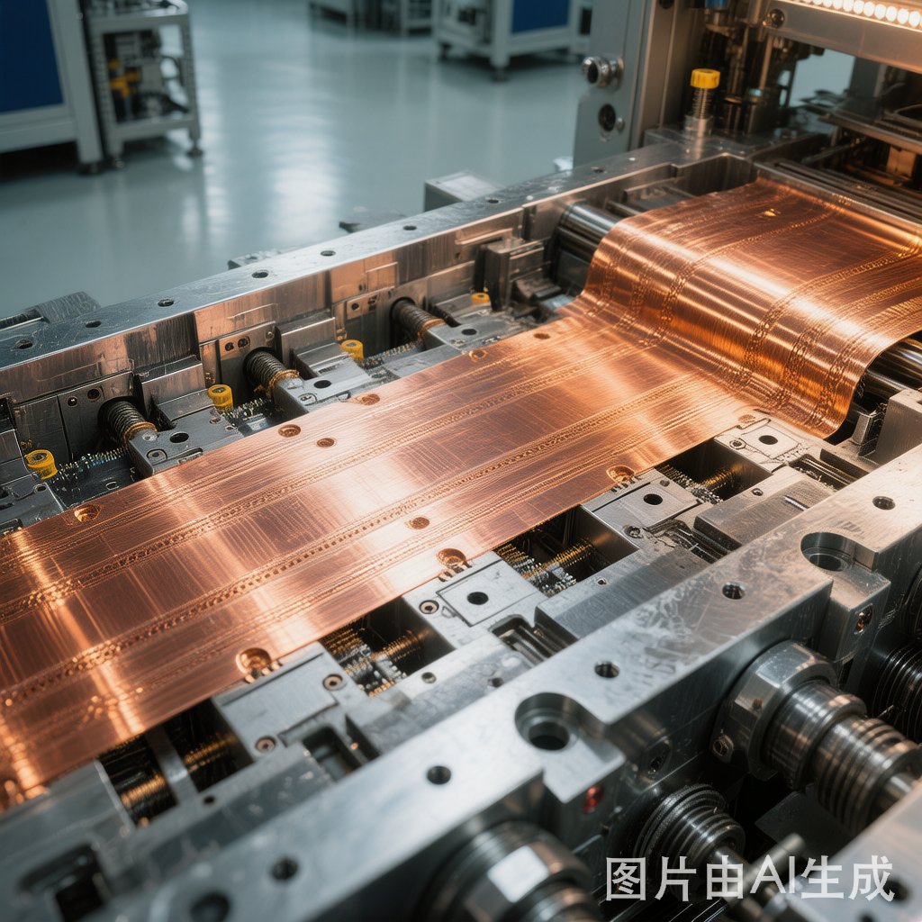
Progressive Die Stamping: The Industry Standard
For high-volume SMT component production, progressive die stamping dominates. A single die set performs multiple operations — piercing, blanking, bending, coining — as the copper strip advances through successive stations. Key advantages include:
- Consistent precision: Typical tolerances of ±0.025 mm (±0.001 inch) are achievable on critical features
- High throughput: Modern presses run at 200–1,200 strokes per minute depending on part complexity
- Material efficiency: Optimized strip layouts achieve 75–85% material utilization
- Integrated features: Embossed standoffs, coined surfaces, and formed spring fingers can all be produced in a single pass
Material Considerations for SMT Copper Strips
Alloy Selection
The choice of copper alloy significantly influences both stamping behavior and end-use performance:
- C11000 (ETP Copper): 100% IACS conductivity, ideal for bus bars and high-current paths, but limited spring properties
- C26000 (Cartridge Brass): Good formability and moderate strength, commonly used for EMI shield frames where soldering is required
- C52100 (Phosphor Bronze): Excellent spring characteristics and fatigue resistance, preferred for co
ector contacts
- C70250 (Copper-Nickel-Silicon): High strength with good conductivity, increasingly popular in miniaturized co
ectors
Temper and Grain Size
Grain size directly affects surface quality after stamping. Fine-grained material (~0.015 mm) produces smoother edges with less burr formation, critical for SMT coplanarity requirements. For most SMT shielding applications, half-hard (H02) temper offers the best balance of formability and strength.
Critical Quality Parameters
Burr Control
Burr height must typically stay below 10% of material thickness — and below 0.025 mm absolute — to prevent solder bridging and coplanarity issues during reflow. Achieving this requires properly maintained punch-to-die clearance (typically 5–8% of material thickness for copper alloys) and regular tool sharpening schedules.
Flatness and Coplanarity
For SMT components, coplanarity requirements demand that all leads or contact pads lie within a 0.10 mm plane after stamping. Post-stamping leveling operations — roller leveling or press leveling with coining — are often necessary to meet these specifications.
Emerging Trends in Copper Stamping for Electronics
Three trends are reshaping the copper stamping landscape for SMT:
- Micro-stamping: As co
ectors shrink to 0.35 mm pitch and below, stamping dies must achieve unprecedented precision with features under 0.2 mm
- Selective plating integration: Combining stamping with in-die selective plating processes reduces handling steps and improves plating consistency on critical contact areas
- Industry 4.0 monitoring: Real-time force monitoring, acoustic emission sensing, and vision inspection systems integrated into stamping presses enable 100% quality verification without slowing production
Conclusion
Copper strip stamping remains the most cost-effective method for producing precision metal components at SMT volumes. Success depends on careful alloy selection, tight process control of burr and flatness parameters, and adoption of emerging technologies for quality assurance. For procurement teams, partnering with stamping suppliers that invest in progressive die expertise and in-process monitoring is essential to maintaining a reliable SMT supply chain.


