The Role of Bus Bars in Electronics Power Distribution
In power electronics systems — from server power supplies and EV chargers to industrial motor drives and energy storage inverters — distributing hundreds or thousands of amperes from the input stage to multiple load points requires conductors that minimize resistive losses and thermal buildup. While PCB copper traces can handle moderate currents, they quickly become impractical above 50–80A continuous due to the excessive copper thickness and board area needed. This is where bus bars excel.
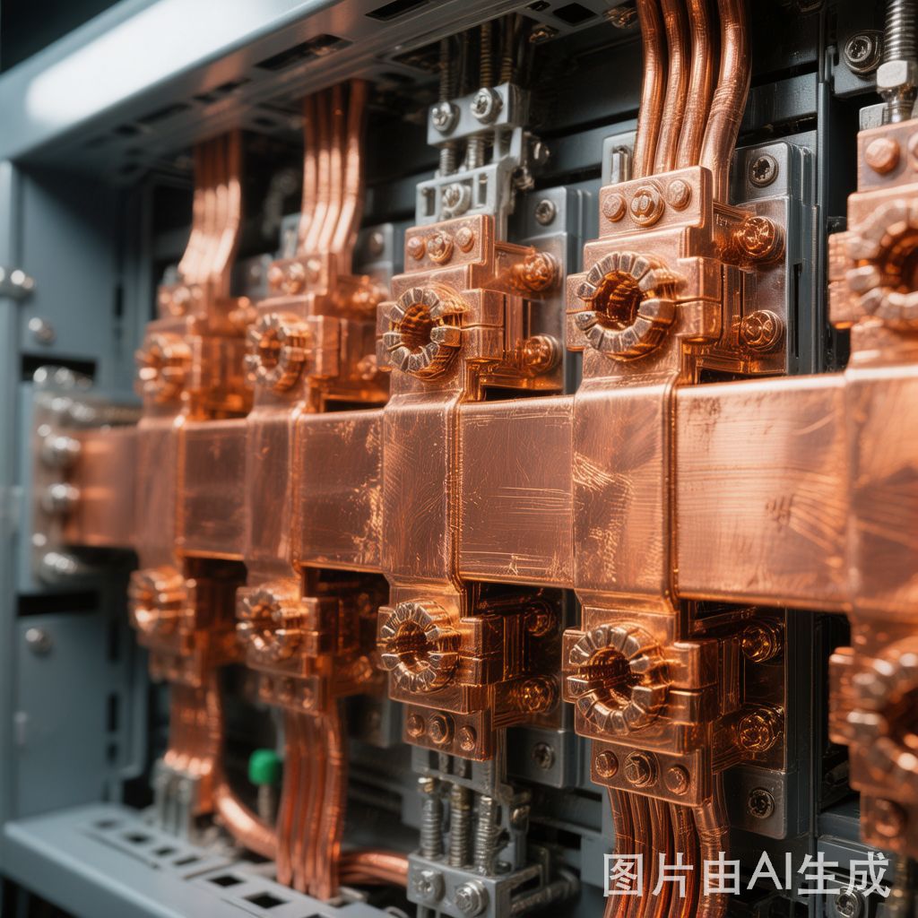
Bare copper bus bars are flat, stamped, or machined copper conductors that carry high currents between power components within an electronics assembly. They replace thick PCB traces and wiring harnesses with a compact, low-inductance, thermally efficient current distribution network.
Selecting the Right Copper Grade
- C101 (OFE Copper, 99.99% Cu): The highest purity copper with the best conductivity (101% IACS). Used in the most demanding applications where every milliohm of resistance matters.
- C110 (ETP Copper, 99.9% Cu): The workhorse grade for electronics bus bars (100% IACS). The most cost-effective choice for most power distribution applications.
- C194 (Copper-Iron Alloy): Contains 2.1–2.6% iron and phosphorus for added strength. Conductivity drops to 75–80% IACS, but higher yield strength allows thi
er bus bars. Commonly used in co
ector terminals.
Cross-Section Design: Balancing Current, Loss, and Temperature
The bus bar cross-section determines its current-carrying capacity, resistance, and weight:
- Resistance: R = ρ × L / A. Doubling the cross-section halves the resistance.
- Current capacity: 2–4 A/mm² for natural convection cooling and 5–8 A/mm² with forced air cooling.
- Temperature rise: Bus bars should not exceed a 30°C rise above ambient per IEC standards.
The optimal cross-section is often a flat, rectangular shape with a width-to-thickness ratio of 5:1 to 10:1. A 10mm × 2mm cross-section handles approximately 40–60A, while 20mm × 3mm handles 80–120A.
To Plate or Not to Plate: The Bare Copper Decision
Bare copper bus bars offer the lowest contact resistance and highest current capacity. However, bare copper oxidizes when exposed to air. Despite this, bare copper remains preferred for SMT bus bars that are soldered directly to the PCB during reflow, because the soldering process cleans the contact surface and creates a metallurgical bond. For bus bars with bolted co
ections, tin or nickel plating is recommended.
SMT-Compatible Bus Bar Design
Mounting Foot Geometry
Solder feet should be 3mm × 3mm to 5mm × 5mm with a solder mask defined (SMD) pad on the PCB. A small dimple or cavity traps solder paste and ensures a reliable fillet after reflow.
Thermal Mass Management
A single bus bar can have 10–50 times the thermal mass of a standard IC package. The reflow profile must extend time above liquidus (TAL) to ensure complete solder wetting.
Stencil Aperture Design
Apply 1.5–2× the standard solder paste volume for bus bar pads to compensate for the large thermal mass absorbing heat during reflow.
Integration with SMT Power Modules
In power electronics modules, bare copper bus bars co
ect power semiconductors (MOSFETs, IGBTs, SiC transistors) to input/output capacitors, DC bus links, and co
ector terminals. For SiC and GaN modules operating above 100kHz, the low inductance of bus bar interco
ects (typically 2–10nH) is critical for reducing voltage overshoot and switching losses.
Manufacturing Considerations for Southeast Asian EMS
Contract manufacturers in Vietnam, Thailand, and the Philippines increasingly handle power electronics assembly with bus bar integration. Key capabilities include precision stamping/etching, automated pick-and-place with high-lift vacuum grippers, and modified reflow profiles.
Conclusion
Bare copper bus bars offer the most efficient power distribution solution for high-current electronics. By selecting the appropriate copper grade, optimizing cross-section geometry, and designing for SMT compatibility, engineers can create compact, reliable power distribution networks that handle hundreds of amperes with minimal losses.


